Photoluminescence LED display device and manufacturing method thereof

A technology of photoluminescence and display devices, applied in identification devices, instruments, etc., can solve the problems of increasing mass production of red and green fluorescent materials arranged side by side, poor alignment, difficult control of the manufacturing process, etc., and achieve improved light energy The effect of using efficiency, increasing the tolerance error of alignment, and avoiding uneven thickness

Pending Publication Date: 2018-12-04
MAVEN OPTRONICS CO LTD
View PDF14 Cites 1 Cited by
  • Summary
  • Abstract
  • Description
  • Claims
  • Application Information

AI Technical Summary

Problems solved by technology

[0007] However, in mobile display devices, the pixels have tiny sizes. Taking a smartphone as an example, when it is equipped with a 5-inch Full HD (High Definition) display device, the length and width of each pixel are 57 microns and 57 microns respectively. 19 microns, these red and green fluorescent materials that are small in size and arranged side by side require a very high alignment accuracy during manufacture, so there is considerable manufacturing difficulty; for example, the green fluorescent material will The red fluorescent material covering the side is partially accumulated on it, making the process difficult to control and resulting in uneven thickness of the fluorescent material
[0008] On the other hand, because the

Method used


Image

  • Photoluminescence LED display device and manufacturing method thereof
  • Photoluminescence LED display device and manufacturing method thereof
  • Photoluminescence LED display device and manufacturing method thereof

Examples


Embodiment Construction

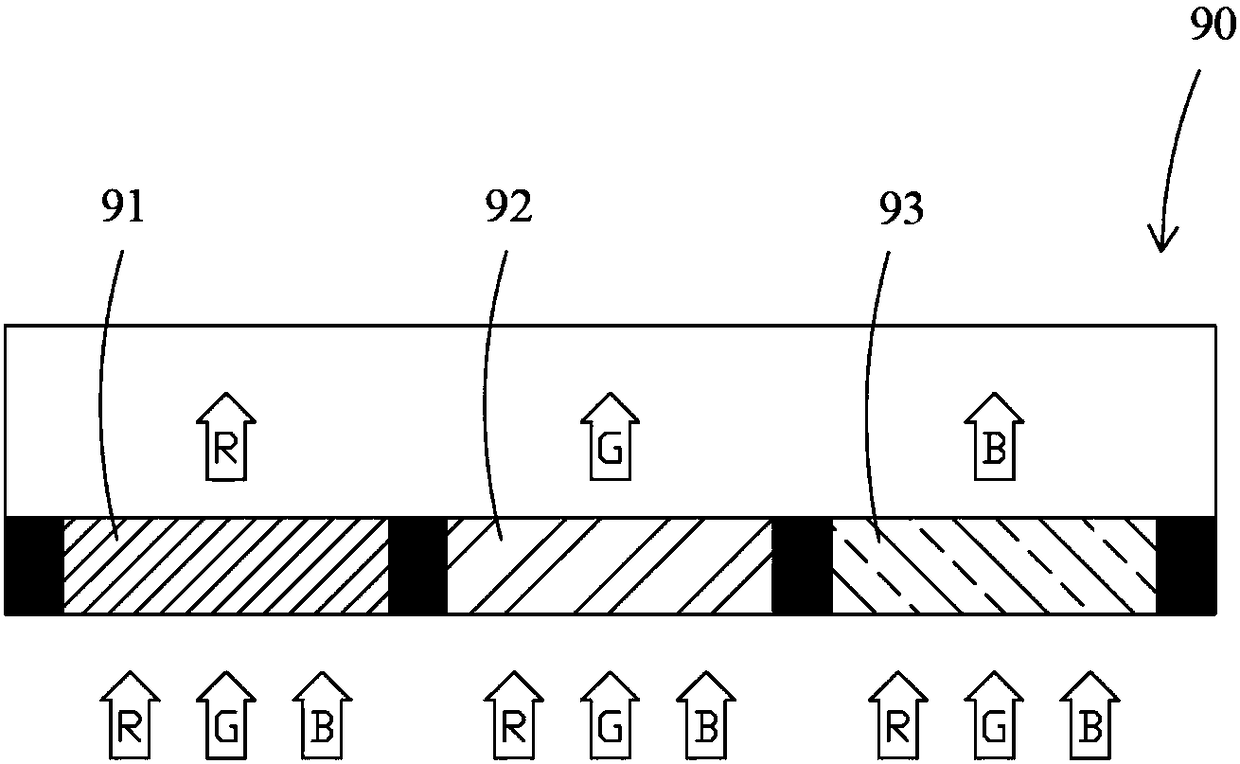
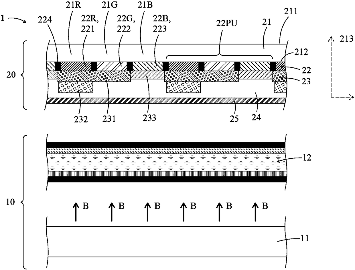
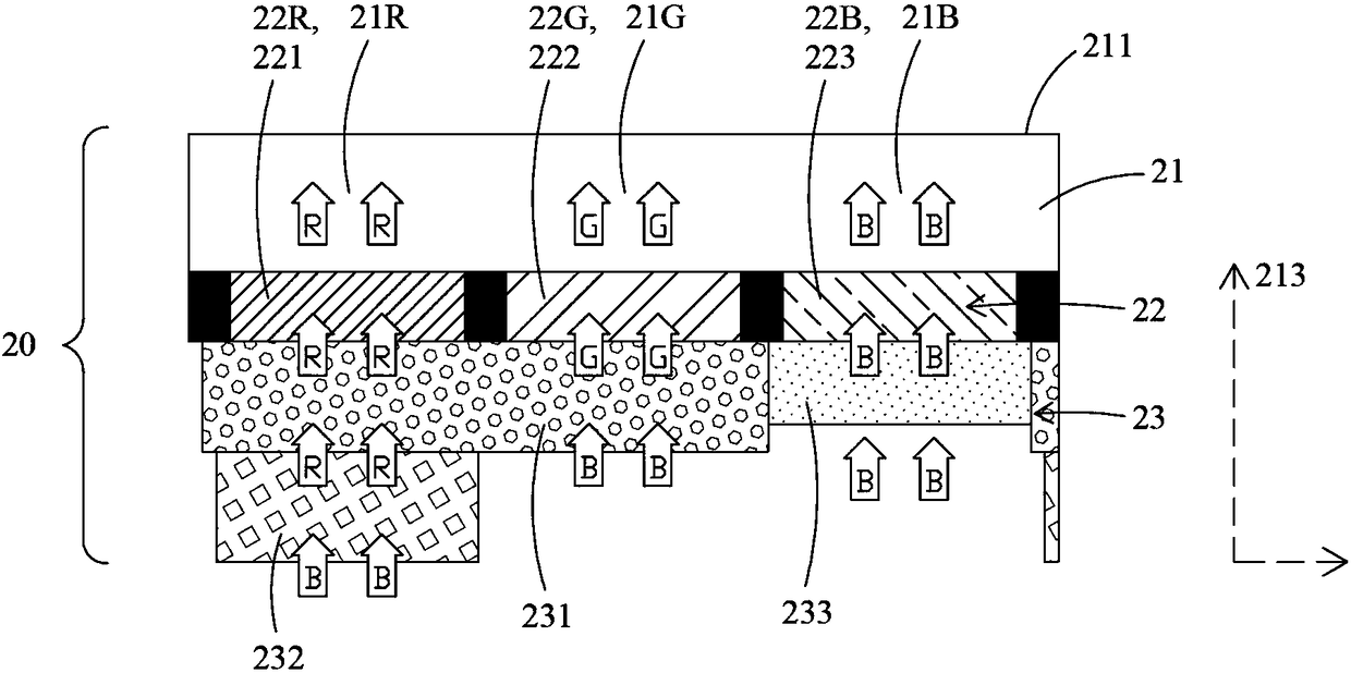
[0075] see Figure 2A FIG. 1 is a schematic diagram of a photoluminescent (PL) display device 1 according to a first preferred embodiment of the present invention. The photoluminescent LED display device 1 (hereinafter referred to as PL display device 1) can provide red pixels formed by red light, green pixels formed by green light and blue pixels formed by blue light, and on the display device A color image is formed. The PL display device 1 can include a blue light source 10 and a display panel 20, the display panel 20 is arranged on one side of the blue light source 10 (for example, the light output side), and the display panel 20 and the blue light source 10 can be separated, or touch. The technical content of the blue light source 10 and the display panel 20 will be further described as follows.

[0076] The blue light source 10 can generate a blue light B, and can make the blue light B evenly illuminate a specific area of ​​the display panel 20, that is, when the disp...


PUM


Abstract

The invention provides a photoluminescence LED display device and a manufacturing method thereof. The display device comprises a light emitting diode array and a display panel which is arranged at oneside of the light emitting diode array, and the display panel comprises a light-transmitting base plate and a photoluminescence layer structure. The photoluminescence layer structure is supported bythe light-transmitting base plate, and the light-transmitting base comprises comprises a red light penetrating area, a green light penetrating area and a blue light penetrating area; the photoluminescence layer structure comprises a red photoluminescence layer and a green photoluminescence layer, wherein the red photoluminescence layer is arranged on the green photoluminescence layer. Therefore, by arranging the photoluminescence layers in a vertical stacked mode, precise pixel positioning of the photoluminescence layer structure can be avoided, so that the display device can be manufactured more easily; and meanwhile, the display device is also relatively excellent in light energy utilization rate and relatively large in display view angle.

Description

technical field [0001] The present invention relates to a display device and a manufacturing method thereof, in particular to a photoluminescent LED display device and a manufacturing method thereof. Background technique [0002] A traditional liquid crystal display device includes a backlight module and a liquid crystal panel, wherein the liquid crystal panel includes a thin film transistor control circuit layer, a liquid crystal layer, a polarizer, a color filter and other components, and the backlight module can produce A white light is sent to the liquid crystal panel, and then the white light can reach the color filter after passing through the liquid crystal layer controlled by the thin film transistor. Such as figure 1 As shown, the color filter 90 includes a red pixel area 91, a green pixel area 92 and a blue pixel area 93, which respectively allow light R with a red spectrum, light G with a green spectrum, and light with a blue spectrum in the white light spectrum....

Claims


Application Information

Patent Timeline
IPC IPC(8): G09F9/33
CPCG09F9/33
Inventor 陈杰
Owner MAVEN OPTRONICS CO LTD
Why Eureka
Try Eureka