Array substrate and preparation method thereof, and display device

A technology of array substrate and substrate substrate, applied in optics, instruments, electrical components, etc., can solve the problems of liquid crystal pixel electrode voltage not being maintained, affecting display effect, etc.

Active Publication Date: 2019-01-01
BOE TECH GRP CO LTD +1
View PDF16 Cites 10 Cited by
  • Summary
  • Abstract
  • Description
  • Claims
  • Application Information

AI Technical Summary

Problems solved by technology

In addition, for liquid crystal display products, the existence of leakage current makes the...

Method used


Image

  • Array substrate and preparation method thereof, and display device
  • Array substrate and preparation method thereof, and display device

Examples


Embodiment Construction

[0030] In order to make the above objects, features and advantages of the present invention more comprehensible, the present invention will be further described in detail below in conjunction with the accompanying drawings and specific embodiments.

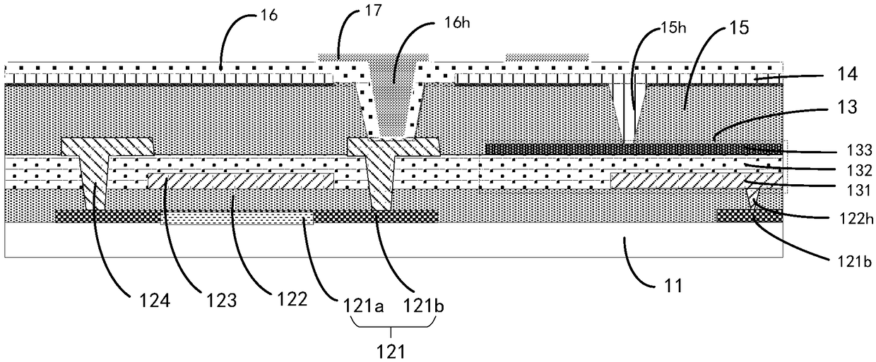
[0031] An embodiment of the present application provides an array substrate, the array substrate may include a plurality of pixel units, and each pixel unit is divided into a light-transmissive area and a reflective area, refer to figure 1 The array substrate in the reflective area includes: a base substrate 11, a thin film transistor disposed on the base substrate 11, and a storage capacitor 13; the storage capacitor 13 includes a metal layer 131 stacked on one side of the base substrate 11, an interlayer dielectric layer 132 and a reflective layer 133, the metal layer 131 is disposed close to the base substrate 11; the common electrode layer 14 disposed on the side of the storage capacitor 13 away from the base substrate 11, the ...


PUM


Abstract

The application provides an array substrate and a preparation method thereof, and a display device. The array substrate comprises multiple pixel units and a public electrode layer, wherein the pixel units are divided into a transmitting region and a reflecting region; the array substrate of the reflecting region comprises a substrate, a thin-film transistor and a storage capacitor, wherein the thin-film transistor and the storage capacitor are arranged on the substrate, the storage capacitor comprises a metal layer, an interlayer dielectric layer and a reflecting layer laminated at one side ofthe substrate, and the metal layer is close to the substrate; and the public electrode layer is arranged at one side, far away from the substrate, of the storage capacitor, wherein the reflecting layer is connected with the public electrode layer, and the metal layer is connected with an active layer of the thin-film transistor. Since the ambient light can be reflected through the arrangement ofthe reflecting layer in the reflecting region, the power consumption of the backlight source is reduced; and meanwhile, the storage capacitor formed between the metal layer and the reflecting layer can store the liquid crystal pixel voltage, the voltage variation caused by leakage current is reduced, the liquid crystal pixel potential holding capacity can be effectively increased, and a display effect is improved.

Description

technical field [0001] The present invention relates to the field of display technology, in particular to an array substrate, a preparation method thereof, and a display device. Background technique [0002] Reflective or transflective display has always been an important technology for low-power liquid crystal display. Generally speaking, the power consumption of the backlight accounts for about 70% to 80% of the total power consumption. Reflective or transflective display devices can make full use of ambient light sources, thus saving the power consumption of the backlight. In addition, for liquid crystal display products, the existence of leakage current makes it impossible to maintain the voltage of the liquid crystal pixel electrodes, which affects the display effect. Contents of the invention [0003] The invention provides an array substrate, a preparation method thereof, and a display device, so as to reduce energy consumption and improve display effect. [0004]...

Claims


Application Information

Patent Timeline
IPC IPC(8): G02F1/1362G02F1/1368G02F1/1343G02F1/1333
CPCG02F1/1333G02F1/134309G02F1/136213G02F1/1368H01L27/1255H01L27/1288H01L27/124G02F1/134363G02F1/133555G02F1/13439G02F1/136227G02F2201/121G02F2201/123G02F2202/104G02F2203/02G02F1/13685G02F1/136231
Inventor 薛进进史大为李峰姚磊王文涛徐海峰杨璐候林王金锋李梅方业周
Owner BOE TECH GRP CO LTD
Why Eureka
Try Eureka