
Eureka
For R&D, Eureka makes reading and utilizing patents & technical documents easy.
Eureka AIR
Designed for self-driven R&D workflows. Generate viable solutions, solve complex R&D challenges, empower your innovation with AI.

Eureka Materials
Designed for material experts only. Revolutionize your material R&D, from search, analyze, to developing new materials.

TechResearch
Generate reliable direction feasibility study reports for your R&D in just a few steps.

TechSeek
Discover and master advanced knowledge NOW. Basics, ideas, possibilities, all at once.

TechMind
As an expert in R&D Theories, TechMind can generates customized viable solutions instantly.

TechRisk
Analyze your overall solution with one click, know your potential R&D risks in advance.

TechMonitor
Get weekly tech updates, stay abreast of the latest tech innovations and key insights.
Chip packaging and positioning clamp
A technology for positioning fixtures and chip packaging, applied in manufacturing tools, workpiece clamping devices, etc., can solve problems such as insufficient accuracy of alignment holes, and achieve the effect of precise positioning and correction
- Summary
- Abstract
- Description
- Claims
- Application Information
AI Technical Summary
Problems solved by technology
Method used
Image

Examples
Embodiment Construction
[0022] The present invention is further described in conjunction with the following examples.
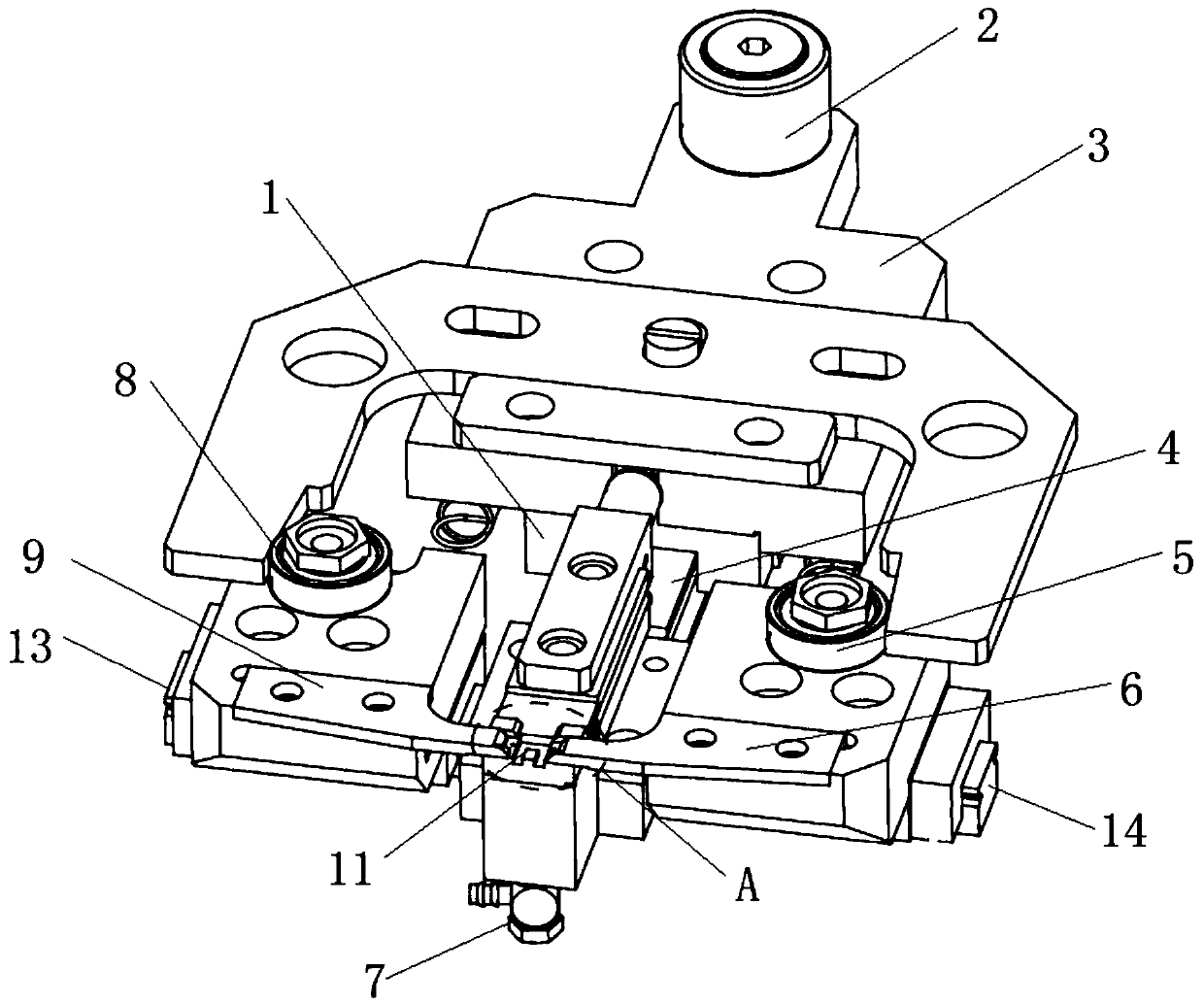
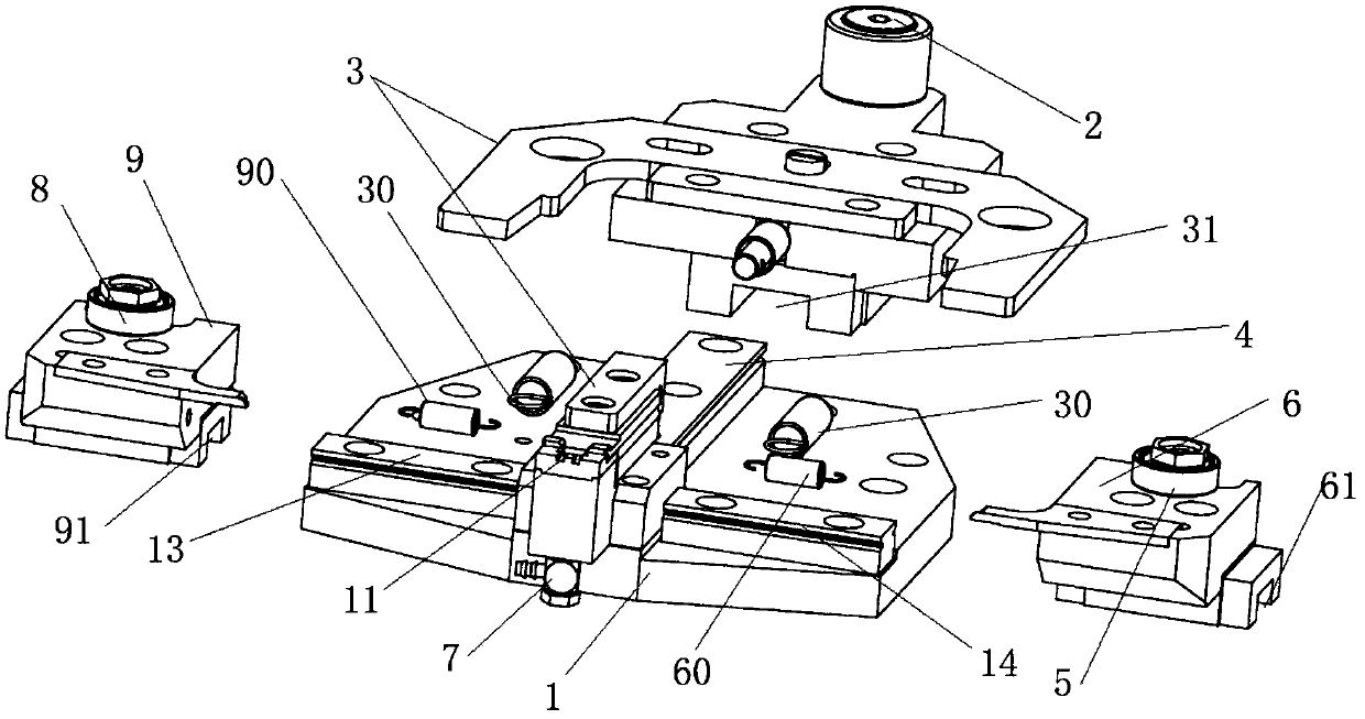
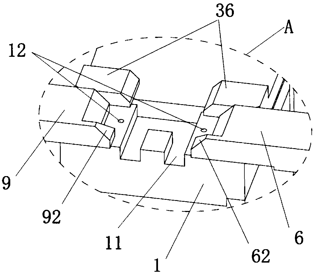
[0023] Such as Figure 1~4 As shown, the chip package positioning fixture includes a base 1 and a chip mounting position 11 arranged on the base 1. A height adjustment member 7 is installed below the chip mounting position 11 to adjust the height of the chip mounting position 11. The base 1 is provided with a longitudinal The slide rail 4 and the horizontal slide rail, the horizontal slide rail is divided into a left slide rail 13 and a right slide rail 14 with the chip mounting position 11 as a node, and the chip mounting position 11 is arranged at the intersecting position of the vertical slide rail 4 and the horizontal slide rail. It also includes a longitudinal jaw 3 and two oppositely arranged transverse jaws, the left jaw 9 and the right jaw 6 which are arranged axially symmetrically with the longitudinal jaw 3 for these two transverse jaws, and are used to drive the longitudi...
PUM
 Abstract
Description
Claims
Application Information
 - R&D Engineer
- R&D Manager
- IP Professional
- Industry Leading Data Capabilities
- Powerful AI technology
- Patent DNA Extraction
Browse by: Latest US Patents, China's latest patents, Technical Efficacy Thesaurus, Application Domain, Technology Topic, Popular Technical Reports.
© 2024 PatSnap. All rights reserved.Legal|Privacy policy|Modern Slavery Act Transparency Statement|Sitemap|About US| Contact US: help@patsnap.com