Display substrate, manufacturing method thereof and display device

A technology for display substrates and substrate substrates, which is applied in the manufacture of semiconductor/solid-state devices, diodes, semiconductor devices, etc., can solve the problems of narrow color gamut of display devices, and achieve the effect of wide color gamut and reduced half-peak width.

Active Publication Date: 2019-07-23
BEIJING BOE TECH DEV CO LTD +1
View PDF3 Cites 3 Cited by
  • Summary
  • Abstract
  • Description
  • Claims
  • Application Information

AI Technical Summary

Problems solved by technology

[0006] Embodiments of the present invention provide a display substrate, a manufacturing method thereof, and a display device, which can solve the problem of a narrow color gamut of the display device

Method used


Image

  • Display substrate, manufacturing method thereof and display device
  • Display substrate, manufacturing method thereof and display device
  • Display substrate, manufacturing method thereof and display device

Examples


Embodiment Construction

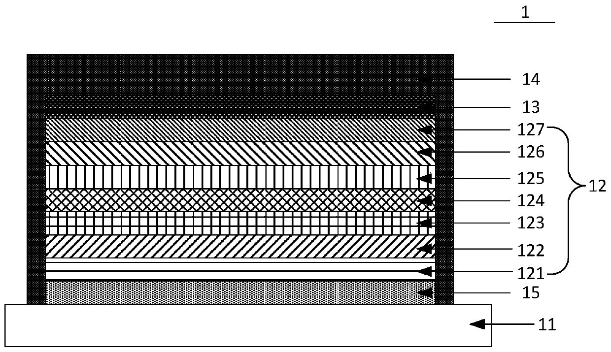
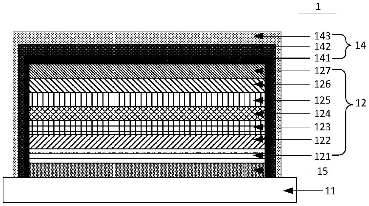
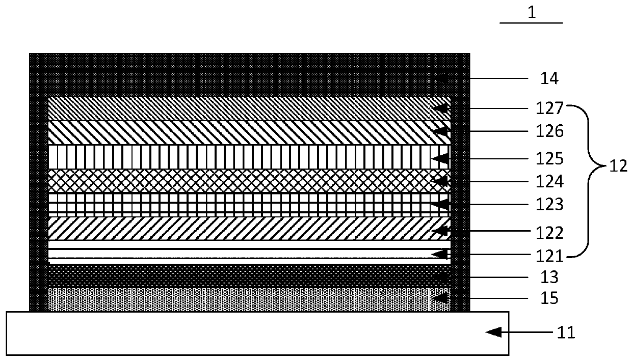
[0052] In order to make the object, technical solution and advantages of the present invention clearer, the present invention will be further described in detail below in conjunction with the accompanying drawings. Obviously, the described embodiments are only some embodiments of the present invention, rather than all embodiments . Based on the embodiments of the present invention, all other embodiments obtained by persons of ordinary skill in the art without making creative efforts belong to the protection scope of the present invention.

[0053]With the continuous development of quantum dot technology, cadmium-based quantum dots are gradually replaced by cadmium-free quantum dots, for example, cadmium-based quantum dots are replaced by indium phosphide (InP) quantum dots. The synthesis process of quantum dots usually includes a nucleation process and a growth process. The nucleation process is isolated from the growth process, and the particle size of the quantum dots can be...


PUM


Abstract

The invention relates to a display substrate, a manufacturing method thereof and a display device, and belongs to the technical field of display. The display substrate comprises a substrate body, an electroluminescent device layer arranged on the substrate body and a light absorption layer arranged on the light emitting side of the electroluminescent device layer, and the half-peak width of the emission spectrum of the electroluminescent device layer is larger than a target width threshold value; wherein the light absorption layer is configured to absorb light rays of a target wavelength, andthe difference value of the target wavelength and the peak wavelength of the emission spectrum is greater than a target difference value threshold value, so that the half-peak width of the emission spectrum of the display substrate is reduced. According to the invention, the display device has a wider color gamut.

Description

technical field [0001] The invention relates to the field of display technology, in particular to a display substrate, a manufacturing method thereof, and a display device. Background technique [0002] With the continuous development of quantum dot technology, the working stability and luminous efficiency of quantum dots are constantly improving, so quantum dot light emitting diode (Quantum Dot Light Emitting Diodes, QLED) display devices are more and more used in people's life. [0003] The traditional quantum dots are cadmium-based quantum dots (quantum dots made of metal cadmium, which is a heavy metal that is easy to cause environmental pollution). With the development of social environmental protection concepts, QLED display devices are developing in the direction of environmental protection. , cadmium-based quantum dots are gradually replaced by cadmium-free quantum dots, for example, cadmium-based quantum dots are replaced by indium phosphide (InP) quantum dots (InP ...

Claims


Application Information

Patent Timeline
Patent Type & Authority Applications(China)
IPC IPC(8): H01L51/52H01L51/56H01L27/32
CPCH10K59/12H10K50/865H10K59/1201H10K71/00H10K59/38H10K50/115H10K50/844
Inventor 陈卓尹思懿
Owner BEIJING BOE TECH DEV CO LTD
Why Eureka
Try Eureka