
White organic light emitting device and color display apparatus employing the same

a technology of light emitting device and color display device, which is applied in the direction of discharge tube/lamp details, discharge tube luminescnet screens, other domestic articles, etc., can solve the problems of disadvantageous white light extraction, difficult realization of large surface and high resolution display devices, and unnecessarily complicated manufacturing processes, etc., to achieve wide color gamut and improve light output efficiency

Active Publication Date: 2009-04-16
SAMSUNG DISPLAY CO LTD
View PDF10 Cites 34 Cited by
  • Summary
  • Abstract
  • Description
  • Claims
  • Application Information

AI Technical Summary

Benefits of technology

[0013]It is another object of the present invention to provide a top emission type white organic light emitting device (OLED) having improved light output efficiency and a wide color gamut, by simply realizing multiple resonating modes.

Problems solved by technology

Forming organic light emitting layers separately for each sub-pixel, however, causes manufacturing processes to become unnecessarily be more complicated, making the realization of a large surface and high resolution display device difficult.
Resonance generated in such a resonance cavity narrows spectrums of light emitted to the exterior, and thus being advantageous in terms of extracting light of a predetermined wavelength only, but disadvantageous in terms of extracting white light.
Accordingly, in order to manufacture a color display apparatus using such OLED, the optical thickness of the resonance cavity should be varied according to sub-pixels of each color, and this, in return, further complicates the manufacturing process.

Method used


Image

  • White organic light emitting device and color display apparatus employing the same
  • White organic light emitting device and color display apparatus employing the same
  • White organic light emitting device and color display apparatus employing the same

Examples


Embodiment Construction

[0042]The present invention will now be described more fully with reference to the accompanying drawings, in which exemplary embodiments of the invention are shown. In the drawings, like reference numerals denote like elements, and the size of the elements may be exaggerated for clarity and convenience of description.

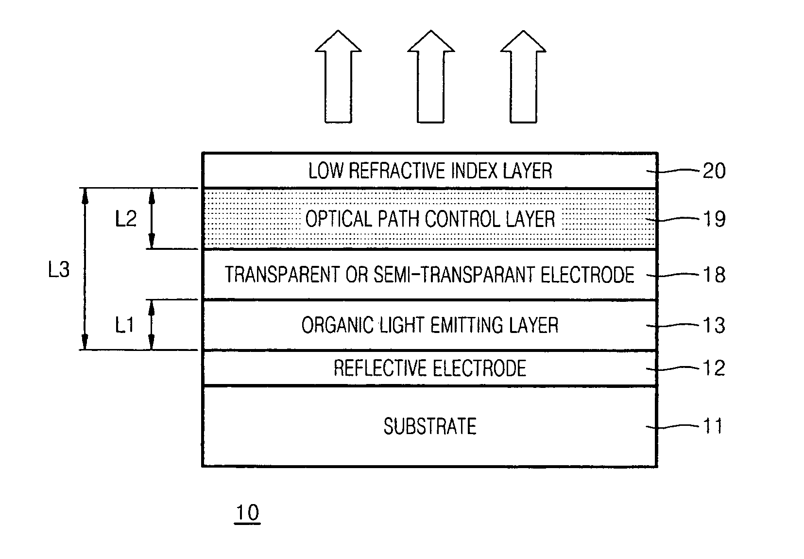
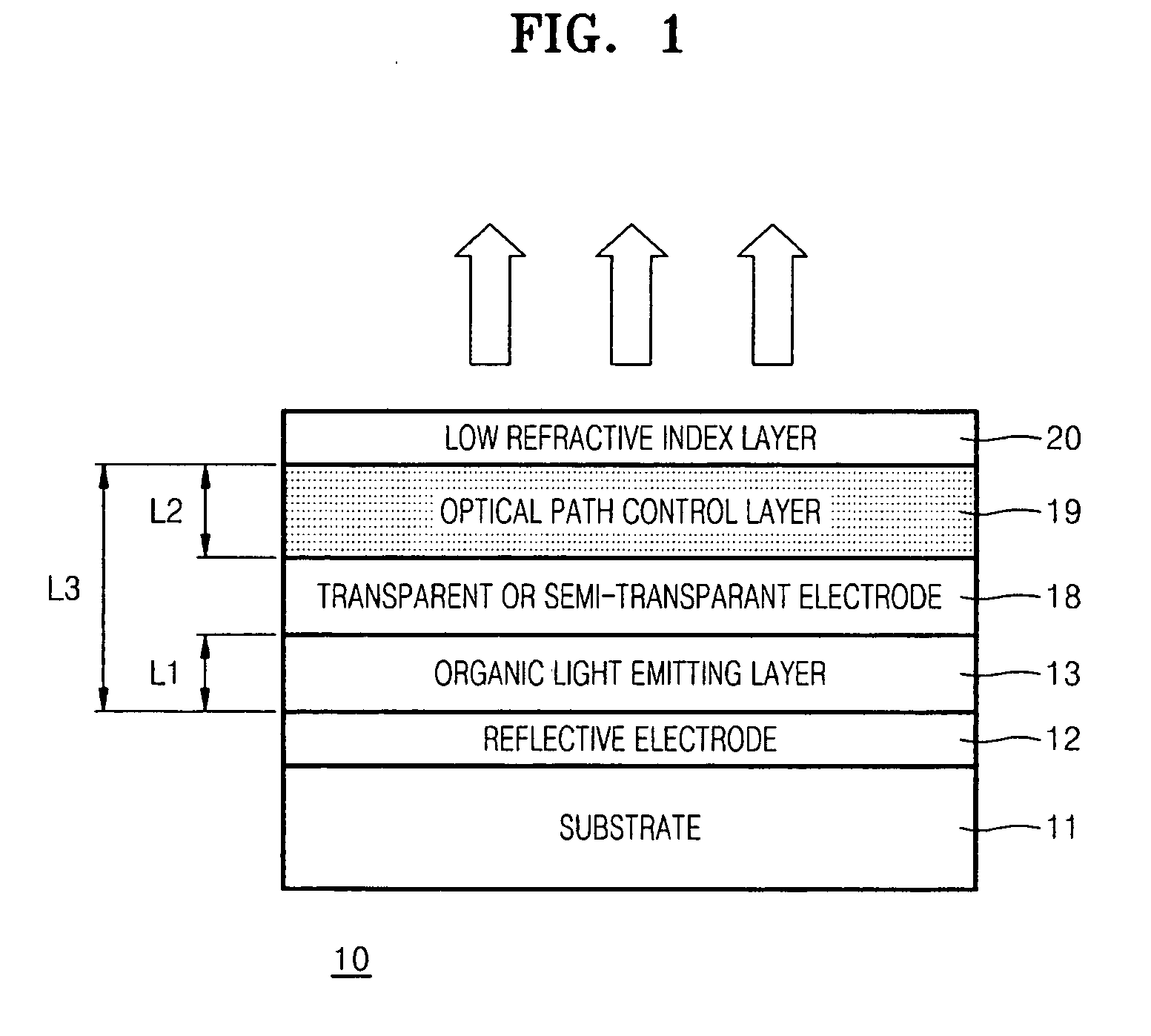
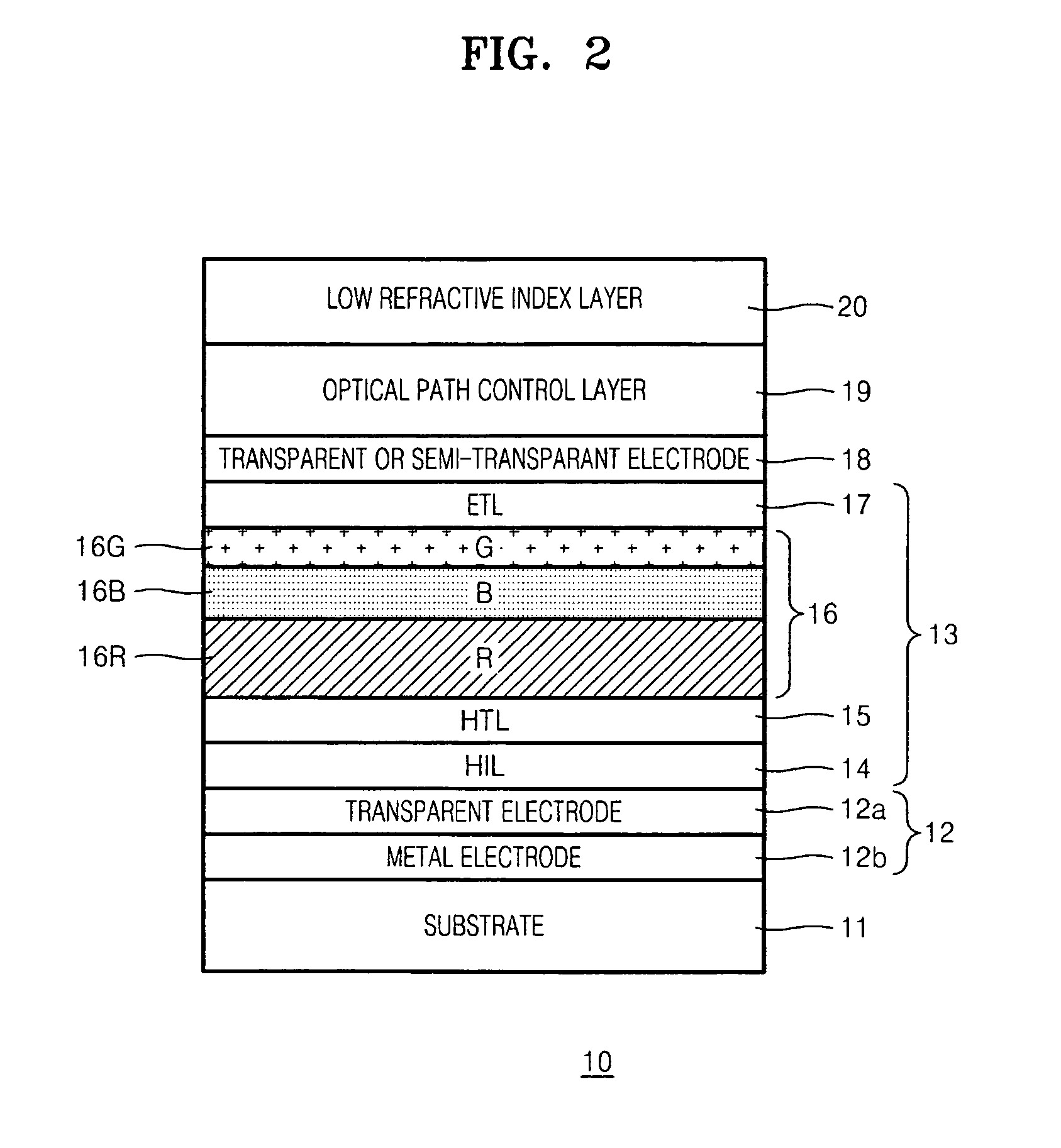
[0043]FIG. 1 is a schematic view of a top emission type white organic light emitting device (OLED) 10, according to an embodiment of the present invention. Referring to FIG. 1, white OLED 10 includes a reflective electrode 12, an organic light emitting layer 13, a semi-transparent or transparent electrode 18, an optical path control layer 19, and a low refractive index layer 20 sequentially stacked on a substrate 11. Substrate 11 may be formed of glass, and a thin film transistor (TFT) may be formed on substrate 11 to control the operation of light emission of organic light emitting layer 13. Organic light emitting layer 13 may have a light emitting structure of a gener...


PUM


Abstract

An organic light emitting device (OLED) having increased light output efficiency and a wide color gamut, and a color display apparatus employing the OLED, includes: a substrate; a reflective electrode formed on the substrate; an organic light emitting layer formed on the reflective electrode; a semi-transparent or transparent electrode formed on the organic light emitting layer; and an optical path control layer formed on the semi-transparent or transparent electrode and formed of a light transmitting material. In the OLED, resonators are formed between the reflective electrode and the semi-transparent or transparent electrode, between the reflective electrode and the top surface of the optical path control layer, and between the top surface of the semi-transparent or transparent electrode and the top surface of the optical path control layer, respectively, therefore, as an optical mode output to the exterior of the optical path control layer, at least two multiple resonances are generated.

Description

CLAIM OF PRIORITY[0001]This application makes reference to, incorporates the same herein, and claims all benefits accruing under 35 U.S.C. §119 from an application for PLASMA DISPLAY PANEL WITH IMPROVED BARRIER RIB STRUCTURE earlier filed in the Korean Intellectual Property Office on Oct. 16, 2007 and there duly assigned Serial No. 10-2007-0104029.BACKGROUND OF THE INVENTION[0002]1. Field of the Invention[0003]The present invention relates to a white organic light emitting device (OLED) and a color display apparatus using the same, and more particularly, to a top emission type white OLED realizing high resolution and having a wide color gamut, and a color display apparatus using the same.[0004]2. Description of the Related Art[0005]An organic light emitting device (OLED) is a display device which forms images by emitting light when holes supplied from an anode and electrons supplied from a cathode are combined in an organic light emitting layer formed between an anode and a cathode....

Claims


Application Information

Patent Timeline
Patent Type & Authority Applications(United States)
IPC IPC(8): H01L51/50
CPCH01L27/322Y10S428/917H01L51/5265H01L51/5036H10K59/38H10K50/125H10K50/852H05B33/22H05B33/28
Inventor LEE, SUNG-HUNTAMURA, SHINICHIROKIM, SANG-YEOLKIM, MU-GYEOMSONG, JUNG-BAE
Owner SAMSUNG DISPLAY CO LTD
Learn More