Organic light emitting display device and method of manufacturing the same

a light-emitting display and organic technology, applied in the direction of thermoelectric device junction materials, semiconductor devices, electrical apparatus, etc., can solve the problems of poor light output efficiency, poor color characteristic, and poor light output efficiency of organic light-emitting display devices, so as to maintain color characteristics, simplify the process, and improve the effect of light output efficiency

Active Publication Date: 2014-05-01
LG DISPLAY CO LTD
View PDF13 Cites 22 Cited by
  • Summary
  • Abstract
  • Description
  • Claims
  • Application Information

AI Technical Summary

Benefits of technology

[0013]An aspect of the present invention is directed to an high-resolution organic light emitting display device for realizing excellent light output efficiency, maintaining color characteristic, simplifying a process, and saving the manufacturing cost.

Problems solved by technology

Also, since the organic light emitting display devices do not need a separate backlight, it is possible to lighten and thin the organic light emitting display devices, and the organic light emitting display devices have excellent power consumption compared to LCD devices and the other flat panel display devices.
Furthermore, the organic light emitting display devices are driven with a low direct current (DC) voltage, have a fast response time, and are low in manufacturing cost.
However, due to limitations of mask manufacturing technology, it is difficult to apply the FMM process to a large size and high resolution.
That is, when the organic light emitting display device is applied to a large area, a mask sags due to the weight thereof, and thus, it is difficult to form a desired pattern.
Also, the spread of organic materials increases due to a separated distance between the mask and a deposition portion, and therefore, it is difficult to realize high resolution.

Method used


Image

  • Organic light emitting display device and method of manufacturing the same
  • Organic light emitting display device and method of manufacturing the same
  • Organic light emitting display device and method of manufacturing the same

Examples


Embodiment Construction

[0022]Hereinafter, embodiments of the present invention will be described in detail with reference to the accompanying drawings. Like reference numerals refer to like elements throughout. In the following description, when the detailed description of the relevant known function or configuration is determined to unnecessarily obscure the important point of the present invention, the detailed description is not provided.

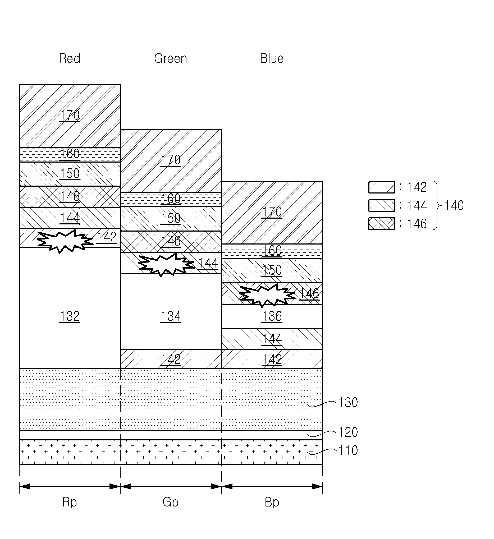
[0023]FIG. 1 is a sectional view schematically illustrating an organic light emitting display device according to an embodiment of the present invention.

[0024]As illustrated in FIG. 1, the organic light emitting display device includes a first electrode (anode) 110, a hole injection layer 120, a first hole transporting layer 130, a second hole transporting layer 132, a third hole transporting layer 134, a fourth hole transporting layer 136, an emitting material layer 140 including first to third emission common layers 142, 144 and 146, an electron transporting layer 15...


PUM


Abstract

Discussed is an organic light emitting display device. The organic light emitting display device includes a substrate in which red, green, and blue pixel areas are defined, a first electrode and a first hole transporting layer that are formed on the substrate, first to third emission common layers formed in each of the pixel areas on the first hole transporting layer, and an electron transporting layer and a second electrode that are formed on the third emission common layer. Accordingly, color mixture is prevented, limitations due to a defective mask are overcome, a process is simplified, and the manufacturing cost is saved.

Description

CROSS-REFERENCE TO RELATED APPLICATIONS[0001]This application claims the benefit of the Korean Patent Application No. 10-2012-0121726 filed on Oct. 31, 2012, which is hereby incorporated by reference as if fully set forth herein.BACKGROUND[0002]1. Field of the Invention[0003]The present invention relates to an organic light emitting display device and a method of manufacturing the same.[0004]2. Discussion of the Related Art[0005]As a type of new flat panel display device, organic light emitting display devices are self-emitting display devices, and have a better viewing angle and contrast ratio than liquid crystal display (LCD) devices. Also, since the organic light emitting display devices do not need a separate backlight, it is possible to lighten and thin the organic light emitting display devices, and the organic light emitting display devices have excellent power consumption compared to LCD devices and the other flat panel display devices. Furthermore, the organic light emittin...

Claims


Application Information

Patent Timeline
Patent Type & Authority Applications(United States)
IPC IPC(8): H01L51/00H01L51/52
CPCH01L51/0001H01L51/52H01L51/5203H10K59/35H10K50/156H10K50/155H10K50/852H10K50/15H10K2102/351H10K50/13H10K50/16H10K50/17H10K50/80H10K50/805H10K50/818H10K50/828H10K50/856H10K71/00H10K71/60
Inventor KIM, MI-NAKIM, KWANG HYUNPARK, JIN HO
Owner LG DISPLAY CO LTD
Why Eureka
Try Eureka