Light emitting device having vertical structure and method for manufacturing the same

a technology of vertical structure and light emitting device, which is applied in the direction of semiconductor/solid-state device manufacturing, semiconductor devices, electrical equipment, etc., can solve the problems of high production cost, low efficiency, and the inability of green leds fabricated using this material to produce pure green light, so as to reduce the etching time for chip regions and prevent damage to semiconductor layers , the effect of easy chip separation

Active Publication Date: 2008-06-19
SUZHOU LEKIN SEMICON CO LTD
View PDF3 Cites 41 Cited by
  • Summary
  • Abstract
  • Description
  • Claims
  • Application Information

AI Technical Summary

Benefits of technology

[0035]An object of the present invention is to provide a light emitting device having a vertical structure and a method for manufacturing the same which are capable of damping impact generated during a substrate separation process using a laser lift off method, and thus, preventing damage of a semiconductor layer, maintaining the ohmic characteristics of electrodes, reducing the etching time for separation of chip regions, and achieving an easy chip separation.

Problems solved by technology

Since GaP is an indirect transition material causing a degradation in efficiency, the green LEDs fabricated using this material cannot practically produce light of pure green.
Despite the rapid advancement in technologies of GaN-based semiconductor devices, the fabrication of GaN-based devices suffers from a great disadvantage of high-production costs.
This disadvantage is closely related to difficulties associated with growing of a GaN thin film (epitaxial layer) and subsequent cutting of finished GaN-based devices.
Meanwhile, since sapphire is an insulating material, available LED devices manufactured using a sapphire substrate (or other insulating substrates) are practically limited to a lateral or vertical structure.
However, the lateral structure or the flip chip method suffers from the problems associated with poor heat release efficiency because the sapphire substrate has a heat conductivity of about 27 W / mK, thus leading to a very high heat resistance.
Furthermore, the flip chip method has also disadvantages of requiring large numbers of photolithography process steps, thus resulting in complicated manufacturing processes.
However, it is impossible to completely remove the sapphire substrate at once, using the LLO method, due to the size and limited uniformity of a laser beam used in the LLO method.
As a result, a degradation in bondability occurs primarily.
In addition, a degradation in electrical characteristics occurs.
Also, during the LLO process, many poor bonding portions may be observed on the thin film.
Furthermore, the above-mentioned method incurs damage of a back surface of the GaN thin film, on which an LED is to be formed, in a region where laser beams overlap with each other.
There may also be a phenomenon that cracks formed at poor-quality portions of the GaN thin film are propagated to other portions of the GaN thin film.
In addition, a plurality of empty spaces causing formation of poor bonding interfaces may be formed.
This air is expanded by high thermal energy of a laser, thereby causing cracks to be formed at the GaN thin film 2 in a region around the trench.
Furthermore, there are adverse affects on the electrical characteristics of the metal layers 3 and 6 used for the fabrication of the GaN-based devices.

Method used


Image

  • Light emitting device having vertical structure and method for manufacturing the same
  • Light emitting device having vertical structure and method for manufacturing the same
  • Light emitting device having vertical structure and method for manufacturing the same

Examples


first embodiment

[0077]Hereinafter, a first embodiment of the present invention will be described with reference to FIGS. 5 to 11.

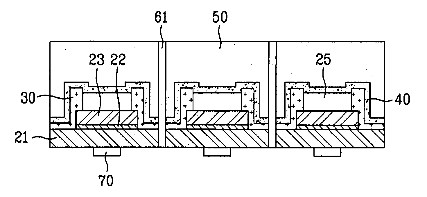
[0078]As shown in FIG. 5, in order to manufacture a light emitting device according to this embodiment, a process for growing a GaN semiconductor layer 20 having a multilayer structure over a sapphire substrate 10 is first carried out.

[0079]The GaN semiconductor layer 20 includes an n type GaN layer 21 formed over the substrate 10, an active layer 22 formed over the n type GaN layer 21, and a p type GaN layer 23 formed over the active layer 22. A separate buffer layer 24 may be formed between the n type GaN layer 21 and the substrate 10.

[0080]The active layer 22 may have a GaN-based single quantum well (SQW) structure, a GaN-based multi-quantum well (MQW) structure, or a quantum structure, for example, a supper lattice of the GaN-based SQW or MQW structure.

[0081]The quantum structure of the active layer 22 may be formed using a combination of various GaN-based materials. ...

second embodiment

[0112]Hereinafter, a second embodiment of the present invention will be described with reference to FIGS. 12 to 18. In the following description, no explanation will be given of the same process as that of the first embodiment.

[0113]As shown in FIG. 12, in order to manufacture a light emitting device according to this embodiment, a process for growing a GaN semiconductor layer 20 having a multilayer structure over a sapphire substrate 10 is first carried out.

[0114]The GaN semiconductor layer 20 includes an n type GaN layer 21 formed over the substrate 10, an active layer 22 formed over the n type GaN layer 21, and a p type GaN layer 23 formed over the active layer 22. A separate buffer layer 24 may be formed between the n type GaN layer 21 and the substrate 10.

[0115]The active layer 22 may have a GaN-based single quantum well (SQW) structure, a GaN-based multi-quantum well (MQW) structure, or a quantum structure, for example, a supper lattice of the GaN-based SQW or MQW structure.

[0...

third embodiment

[0140]Hereinafter, a third embodiment of the present invention will be described with reference to FIGS. 19 and 20.

[0141]As shown in FIG. 19, in order to manufacture a light emitting device according to this embodiment, a process for growing a GaN semiconductor layer 200 having a multilayer structure over a sapphire substrate 100 is first carried out.

[0142]The GaN semiconductor layer 200 includes an n type GaN layer formed over the substrate 100, an active layer formed over the n type GaN layer, and a p type GaN layer formed over the active layer. A separate buffer layer may be formed between the n type GaN layer and the substrate 100.

[0143]Alternatively, a p type GaN layer may be formed over the substrate 100, and an active layer and an n type GaN layer may be sequentially formed over the p type GaN layer.

[0144]The active layer may have a GaN-based single quantum well (SQW) structure, a GaN-based multi-quantum well (MQW) structure, or a quantum structure, for example, a supper latt...


PUM


Abstract

A light emitting device having a vertical structure and a method for manufacturing the same, which are capable of damping impact generated during a substrate separation process and achieving an improvement in mass productivity, are disclosed. The light emitting device includes a semiconductor layer having a multilayer structure, a first electrode arranged at one surface of the semiconductor layer, a metal support arranged on the first electrode, and an impact damping layer arranged between the first electrode and the metal support, and made of a metal having a ductility higher than a ductility of a metal for the metal support.

Description

[0001]This application claims the benefit of Korean Patent Application No. 10-2006-0023538, filed on Mar. 14, 2006, Korean Patent Application No. 10-2006-0023539, filed on Mar. 14, 2006, and Korean Patent Application No. 10-2006-0024152, filed on Mar. 16, 2006, which are hereby incorporated by references as if fully set forth herein.BACKGROUND OF THE INVENTION[0002]1. Field of the Invention[0003]The present invention relates to a light emitting device having a vertical structure and a method for manufacturing the same, and more particularly, to a light emitting device having a vertical structure and a method for manufacturing the same which are capable of damping impact generated in a substrate separation process, and achieving an improvement in mass productivity.[0004]2. Discussion of the Related Art[0005]Light emitting diodes (LEDs) are well known as a semiconductor light emitting device which converts current to light, to emit light. Since a red LED using GaAsP compound semicondu...

Claims


Application Information

Patent Timeline
Patent Type & Authority Applications(United States)
IPC IPC(8): H01L33/00H01L33/62
CPCH01L33/0079H01L2224/24H01L33/62H01L33/0095H01L33/0093
Inventor JANG, JUN HOLEE, HYUN JAE
Owner SUZHOU LEKIN SEMICON CO LTD
Why Eureka
Try Eureka