

Light emitting device having high optical output efficiency
- Summary
- Abstract
- Description
- Claims
- Application Information
AI Technical Summary
Benefits of technology
Problems solved by technology
Method used
Image

Examples
first embodiment
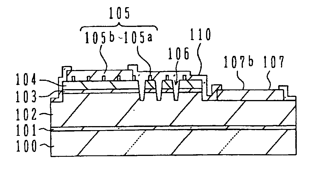
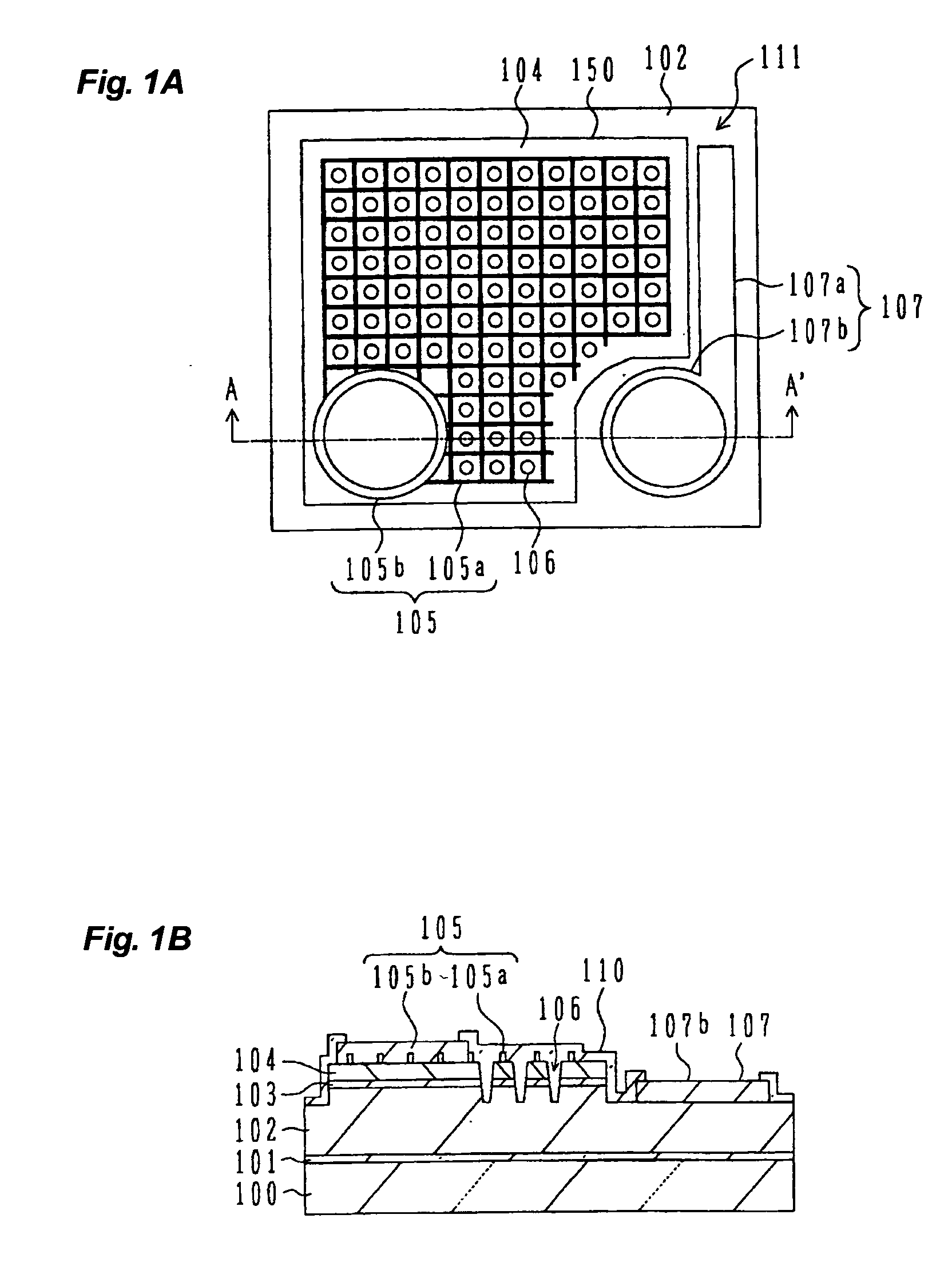
[0056] Next, with reference to FIGS. 1A and 1B, description will be made on a light emitting device according to the present invention.
[0057]FIG. 1A is a schematic plan view of the light emitting device according to the first embodiment, and FIG. 1B is a schematic cross sectional view of the light emitting device of the first embodiment taken along the line A-A′ shown in FIG. 1A.
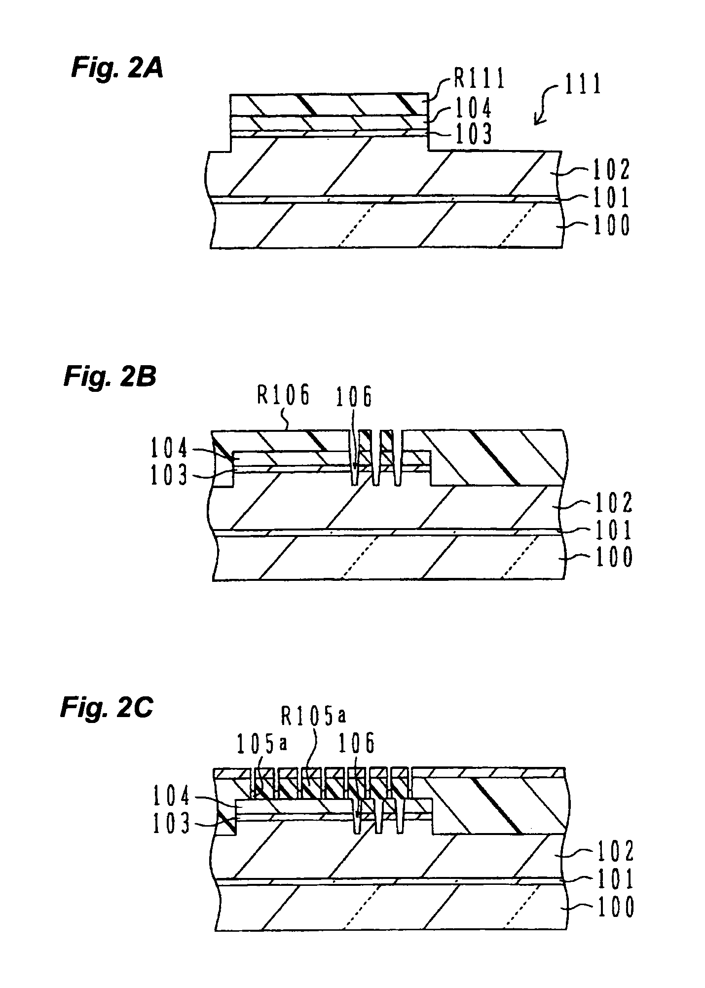
[0058] The nitride semiconductor wafer described with reference to FIG. 19 is used as the material of the light emitting device of this embodiment. An optical emission region 150 is defined on the surface of a p-type nitride semiconductor layer 104, the optical emission region 150 having a square shape with a recess at one corner. The p-type nitride semiconductor layer 104, an optical emission layer 103 and a surface layer of an n-type nitride semiconductor layer 102, in an area surrounding the optical emission area 150, are removed to form a recess 111 (contour groove 111) exposing the n-type nitride semic...
second embodiment
[0170] Next, with reference to FIG. 9B, the operation and effects of the lattice portion 205a of the light emitting device of the second embodiment will be described.
[0171] Consider light emitted from the region of the optical emission layer 103 disposed under the coupling part of the lattice portion 205a. Consider that this region is divided into sub-regions along the longitudinal direction of the coupling part. Light emitted from each divided sub-region along the longitudinal direction of the coupling part is accumulated. It can therefore be considered that light emitted along the longitudinal direction of the coupling part becomes stronger than the light emitted along other directions. Light emitted from the region disposed under the linear portion of the p-side electrode along the longitudinal direction of the linear portion is referred to as “electrode parallel propagating light.”
[0172] The dent 206 disposed in the square part connecting the above-described coupling parts is po...
third embodiment
[0193] There is a tendency that a region of the optical emission layer having a high current density is degraded. In the light emitting device of the third embodiment, current in the optical emission layer can be dispersed so that degradation of the light emitting device can be suppressed.
[0194] Next, with reference to FIGS. 12A to 12C, a light emitting device of a fourth embodiment will be described. FIG. 12A is a schematic plan view of the light emitting device of the fourth embodiment, and FIGS. 12B and 12C are schematic cross sectional views respectively taken along the lines A-A′ and B-B′ shown in FIG. 12A.
[0195] The light emitting device of this embodiment uses a nitride semiconductor wafer similar to that used by the light emitting devices of the first and second embodiments and comparative example.
[0196] In the light emitting device of this embodiment, a region 413 (n-side pad layout region 413) of a contour groove 411 where a pad portion 407b of the n-side electrode 407 i...
PUM
 Abstract
Description
Claims
Application Information