Structure of p-electrode at the light-emerging side of light-emitting diode

a technology of light-emitting diodes and pelectrodes, which is applied in the direction of basic electric elements, electrical apparatus, and semiconductor devices, can solve the problems of difficult to obtain a low-resistance p-type contact layer, the semiconductor itself cannot sufficiently diffuse current, and the difficulty in producing a p-type semiconductor, etc., to achieve the effect of increasing the light transmittance of the p-electrode and increasing the optical output of the led

Inactive Publication Date: 2005-06-07
SUMITOMO ELECTRIC IND LTD
View PDF13 Cites 32 Cited by
  • Summary
  • Abstract
  • Description
  • Claims
  • Application Information

AI Technical Summary

Benefits of technology

[0019]An object of the present invention is to offer an improved structure of the p-electrode in contact with a p-type contact layer of an LED. The improvement is to be attained by increasing the light transmittance of the p-electrode in order to increase the optical output of the LED.

Problems solved by technology

However, when an LED is produced by using a material that makes it difficult to obtain a low-resistance p-type semiconductor, the semiconductor itself cannot sufficiently diffuse the current.
With a GaN- or ZnSe-based wide-bandgap semiconductor, it is difficult to produce a p-type semiconductor, particularly a low-resistance p-type semiconductor.
This is the reason why an LED using such a semiconductor has difficulty in obtaining a low-resistance p-type contact layer.
As a result, the LED cannot be provided with a current-diffusing layer.
With an LED having no current-diffusing layer, the bonding electrode for wire bonding alone cannot diffuse the current sufficiently in the p-type contact layer.
As a result, the effective area of the light-emitting section is decreased, notably decreasing the luminous efficiency.
In addition, the current crowding decreases the life of the LED.
However, although the semi-transparent thin-film metal electrode covering the entire p-type contact layer can transmit light, its transmittance is low.
However, if the metal electrode is excessively thin, the electrical resistance in the lateral direction increases, decreasing the effect of current diffusion by the metal electrode.
For example, when Au is used as the metal electrode, if the thickness is decreased to 5 nm, a sufficient current cannot flow into the Au electrode due to the increased resistance.
The GaN-LED provided with the ITO transparent electrode without using a mesh-shaped metal electrode has a problem in that the junction barrier between the ITO electrode and the n-type contact layer (n-GaN) is so high that the forward voltage drop becomes as high as seven volts.
As a result, a low-voltage drive cannot be performed.

Method used


Image

  • Structure of p-electrode at the light-emerging side of light-emitting diode
  • Structure of p-electrode at the light-emerging side of light-emitting diode
  • Structure of p-electrode at the light-emerging side of light-emitting diode

Examples


Embodiment Construction

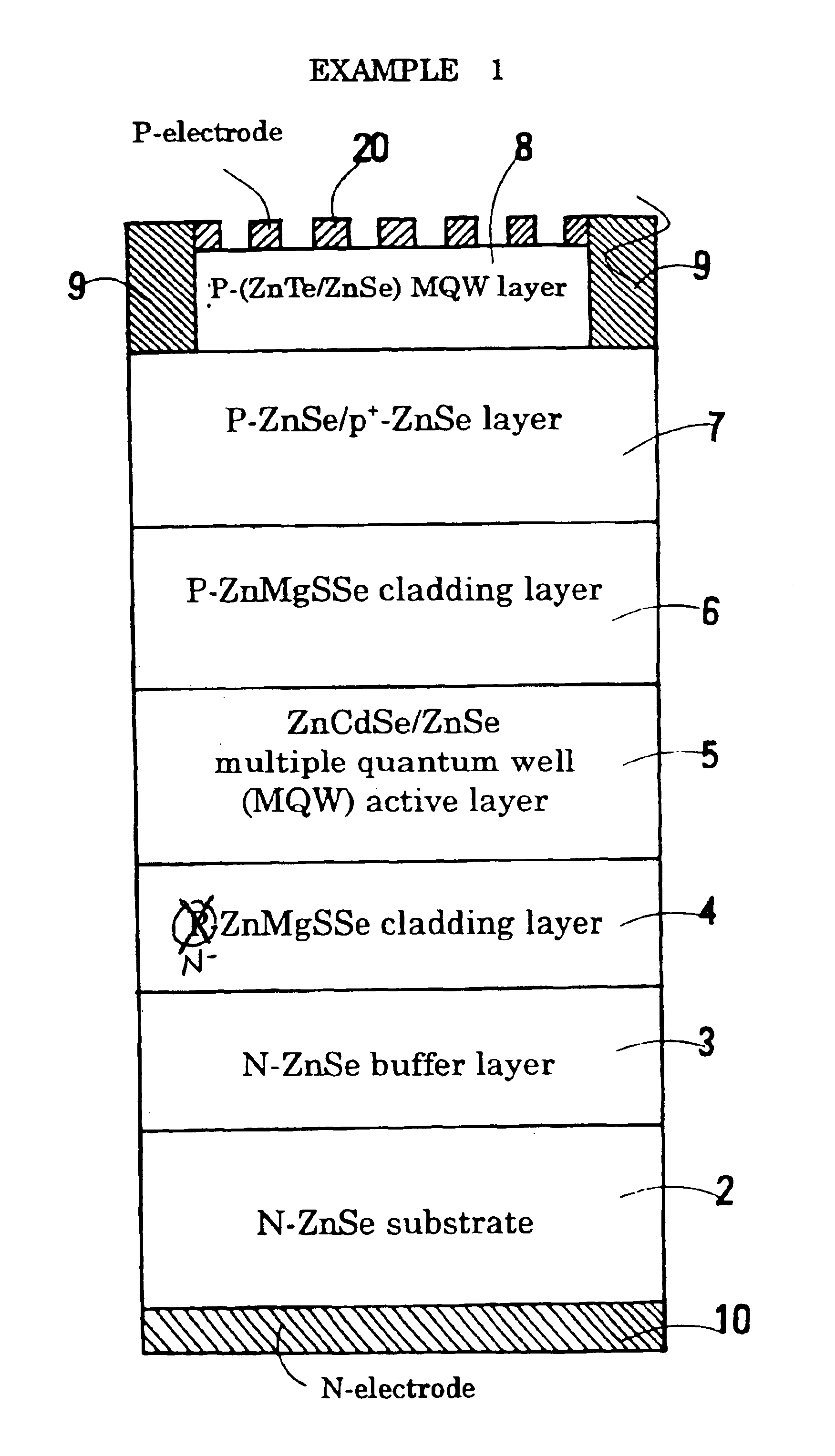
[0111]Embodiments of the present invention are explained below by referring to the accompanying drawings. In the drawings, the same number or sign refers to the same element to avoid duplicated explanation. The ratios of the dimensions in the drawings do not necessarily coincide with the explanation.

[a. Material for the Light-emitting Element]

[0112]The present invention aims at improving an LED that uses ZnSe or GaN, which has a wide bandgap and even when sufficiently doped with impurities, shows high resistivity because of the shortage of charge carriers.

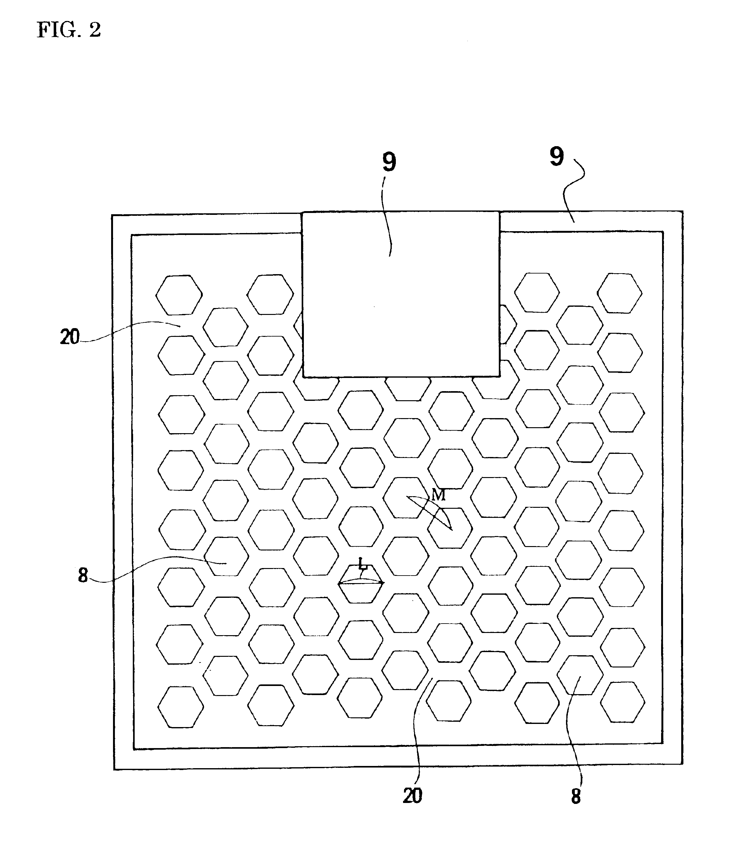
[b. Shape of the Electrode]

[0113]The present invention aims to improve the shape of the p-electrode from which the light emerges.

[c. P-type Contact Layer]

[0114]With a wide-bandgap semiconductor such as ZnSe or GaN, the doping of p-type impurities is not easy. Even if the doping is satisfactorily performed, the activation rate is low, and not many positive holes are excited from the acceptor in many cases. As a result, the p-type ca...


PUM


Abstract

A structure of a p-electrode formed at the light-emerging side of an LED that comprises (a) an n-type semiconductor substrate, (b) an n-type cladding layer, an active layer, a p-type cladding layer, and a p-type contact layer formed on the substrate in this order, and (c) an n-electrode formed on the back face of the substrate. The structure of the p-electrode comprises a mesh-shaped semi-transparent thin-film metal electrode for diffusing electric current formed on the p-type contact layer and a bonding electrode for wire bonding. The metal electrode comprises a covering portion having a transmittance of at least 10% and an opening portion having an opening ratio of at least 20%. The bonding electrode is formed at the periphery of the p-type contact layer and is bonded directly to the mesh-shaped semi-transparent thin-film metal electrode. This structure can increase the intensity of the output light emerging from the p-side.

Description

BACKGROUND OF THE INVENTION[0001]1. Field of the Invention[0002]The present invention relates to a structure of a p-electrode at the light-emerging side of a light-emitting diode, and particularly to a structure of the p-electrode improved so as not to obstruct the passing of light in a light-emitting diode using a wide-bandgap semiconductor such as ZnSe or GaN.[0003]2. Description of the Background Art[0004]A light-emitting diode (hereinafter referred to as LED) has an n-electrode on one of the two main surfaces (top and bottom surfaces) and a p-electrode on the other. In the case of a surface-illuminating-type LED, either surface is used as the light-emerging surface. The electrode, usually made of metal, is required not to obstruct the passing of light.[0005]An LED such as an AlGaAs-based LED has a structure in which a p-type GaAs contact layer, having a sufficient electrical conductivity, is placed on the pn junction, and a small-area dot- or ring-shaped p-electrode is placed on...

Claims


Application Information

Patent Timeline
Patent Type & Authority Patents(United States)
IPC IPC(8): H01L33/00H01L33/06H01L33/12H01L33/28H01L33/32H01L33/38H01L33/42
CPCH01L33/28H01L33/38H01L33/32
Inventor KATAYAMA, KOJI
Owner SUMITOMO ELECTRIC IND LTD
Why Eureka
Try Eureka