Highly reflective mounting arrangement for LEDs

a technology of leds and mounting arrangements, applied in the direction of basic electric elements, electrical apparatus, semiconductor devices, etc., can solve the problems of not providing for high reflectance for light incident, contact absorption still too high to achieve very high light absorption, and increase the chance of reabsorption and loss, so as to improve the overall device light emission and reduce the effect of additional manufacturing costs

Inactive Publication Date: 2009-11-24
KK TOSHIBA
View PDF11 Cites 116 Cited by
  • Summary
  • Abstract
  • Description
  • Claims
  • Application Information

AI Technical Summary

Benefits of technology

[0014]In an alternative embodiment a thick, low index of refraction dielectric, a DBR and a reflective metal stack is deposited on the bottom of the original substrate onto which the LED layers are grown on the other surface. This structure improves the overall device light emission at the lowest possible additional manufacturing cost.

Problems solved by technology

This light is repeatedly reflected, greatly increasing its chance for reabsorption and loss.
Unfortunately, Ag presents a reliability concern because it is subject to tarnish and it is subject to electromigration during device operation.
However, these contacts are still too absorptive to achieve very high light-extraction because the reflectance of metals is limited to below about 93%; in addition, metals suitable for forming an ohmic contact are highly absorbing.
This single dielectric layer serves to improve the reflectance compared to a simple metal reflector, but it does not provide for high reflectance for light incident at high angles, since the dielectric is so thin.
The contact area to the semiconductor is small for these contacts which can significantly increase the resistance to electrical current flow, reducing the overall efficiency of the LED.
Also, since the electrical contact is made in spots the current injection is not uniform over the surface of the chip.
Schubert's data indicates quite good reflectivity; however the process he teaches is complex and has quite tight tolerances requiring very expensive process controls; low yields can be anticipated.

Method used


Image

  • Highly reflective mounting arrangement for LEDs
  • Highly reflective mounting arrangement for LEDs
  • Highly reflective mounting arrangement for LEDs

Examples


Embodiment Construction

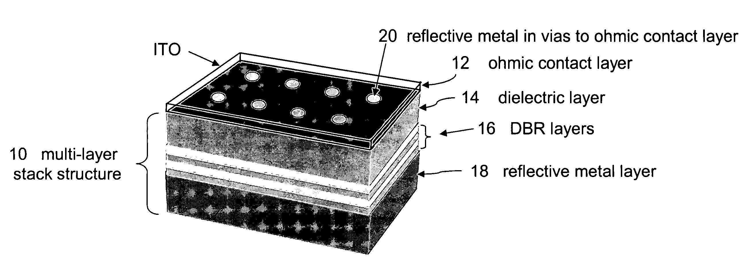
[0022]The present invention is a multi-layer arrangement which provides distinctive improvements over the prior art including, but not limited to, ohmic contacts to an LED, providing high reflectivity for light at all angles, low and, preferably, uniform contact resistance, and improved reliability. FIG. 1 shows a cross-sectional view of one embodiment of the present invention. In particular, FIG. 1 illustrates a stack structure to make ohmic connection to p-type AlInGaN alloys; one embodiment of LED semiconductor layers are shown in FIG. 4. A multilayer structure 10 includes a transparent, ohmic contact layer 12 for making a low-resistance, uniform contact to a p-type semiconductor material, for example AlInGaN. One example of a transparent, ohmic contact layer 12 is ITO, commonly formed by electron beam evaporation and preferably in the range of 50-400 nm thick. The thickness of a transparent, ohmic contact layer 12 is chosen to be sufficiently thick to provide for low-resistance ...


PUM


Abstract

A semiconductor device emitting light about a predetermined wavelength comprising a structure comprising a plurality of layers, sometimes referred to as a stack, providing low resistance, high reflectivity and ohmic contacts to at least one semiconductor material.

Description

FIELD OF THE INVENTION[0001]This invention relates to a reflective submount for light emitting devices (LEDs).CROSS-REFERENCE TO RELATED DOCUMENTS[0002]The present invention is related in part to application Ser. No. 11 / 296,006, “Light Emitter with Metal-oxide Coating” assigned to the same assignee is incorporated herein in its entirety by reference.BACKGROUND OF INVENTION[0003]Light emitting devices (LEDs) emit light in response to excitation by an electrical current. One typical LED includes a heterostructure grown on a substrate by metal-organic vapor phase epitaxy or similar techniques. A LED heterostructure includes n and p type semiconductor layers that sandwich light producing layers. Exemplary light producing layers may be quantum wells surrounded by barrier layers. Typically, electrical contacts are attached to n and p semiconductor cladding layers. When a forward bias is applied across electrical contacts electrons and holes flow from n and p layers into a light producing ...

Claims


Application Information

Patent Timeline
Patent Type & Authority Patents(United States)
IPC IPC(8): H01L31/0232
CPCH01L33/46H01L33/387
Inventor LESTER, STEVEN D.SHUM, FRANKLIN, CHAO-KUNSO, WILLIAMMO, QINGWEI
Owner KK TOSHIBA
Why Eureka
Try Eureka