Light emitting device

a technology of light-emitting devices and light-emitting components, which is applied in the field of light-emitting devices, can solve the problems of increased number of components, high cost, and easy drop in production and supply of plants such as vegetables and fruits, and achieves the effects of brighter light, increased production efficiency, and adequate crystal growth

Active Publication Date: 2015-12-10
SHARP KK
View PDF3 Cites 20 Cited by
  • Summary
  • Abstract
  • Description
  • Claims
  • Application Information

AI Technical Summary

Benefits of technology

[0026]According to the present invention, a light emitting device has a far-red phosphor that, when excited by excitation light from a light emitting element, emits far-red light, and the median size of the far-red phosphor is optimized to be in a range of 1 μm to 20 μm. Providing such a far-red phosphor allows adequate crystal growth, preventing incomplete crystal growth, or abnormal crystal growth resulting in coarse particles. Thus, the light emitting device produces brighter light, and allows more efficient growth of plants. Moreover, a phosphor layer containing the far-red phosphor or the red phosphor is formed to reduce the absorption of the light emitted from the red phosphor by the far-red phosphor. Thus, it improves the light output efficiency of the light emitting device, leading to more efficient growth of plants.

Problems solved by technology

The production and supply of plants such as vegetables and fruits are susceptible to drops due to climatic changes, pest damage, etc.
However, provided with a plurality of light emitting elements, the configuration suffers from a complicated design of the drive circuit to accommodate the electrical and temperature characteristics of the individual light emitting elements, and from high cost resulting from the increased number of components.

Method used


Image

  • Light emitting device
  • Light emitting device
  • Light emitting device

Examples


first embodiment

[0044]Prior to a description of a first embodiment of the present invention, a brief description will be given of the growth of plants. Light acts as a source of stimuli and a source of information in plants' sprouting, flowering, stalk growth, etc. In plants, photosynthesis takes place as a result of chlorophyll absorbing light. The absorption of light by chlorophyll peaks in two wavelength regions, the first being a wavelength range of 400 nm to 500 nm (more specifically, around 450 nm) and the second being a wavelength range of 600 nm to 700 nm (more specifically, around 660 nm).

[0045]Light in the first region (blue light) is necessary for proper morphogenesis of leaves etc., and light in the second region (red light) is necessary for photosynthesis. Moreover, in cases where plants are irradiated with mixed light, far-red light is considered necessary for internode growth and sprout formation. Phytochrome in plants absorbs different types of light by undergoing reversible photoco...

second embodiment

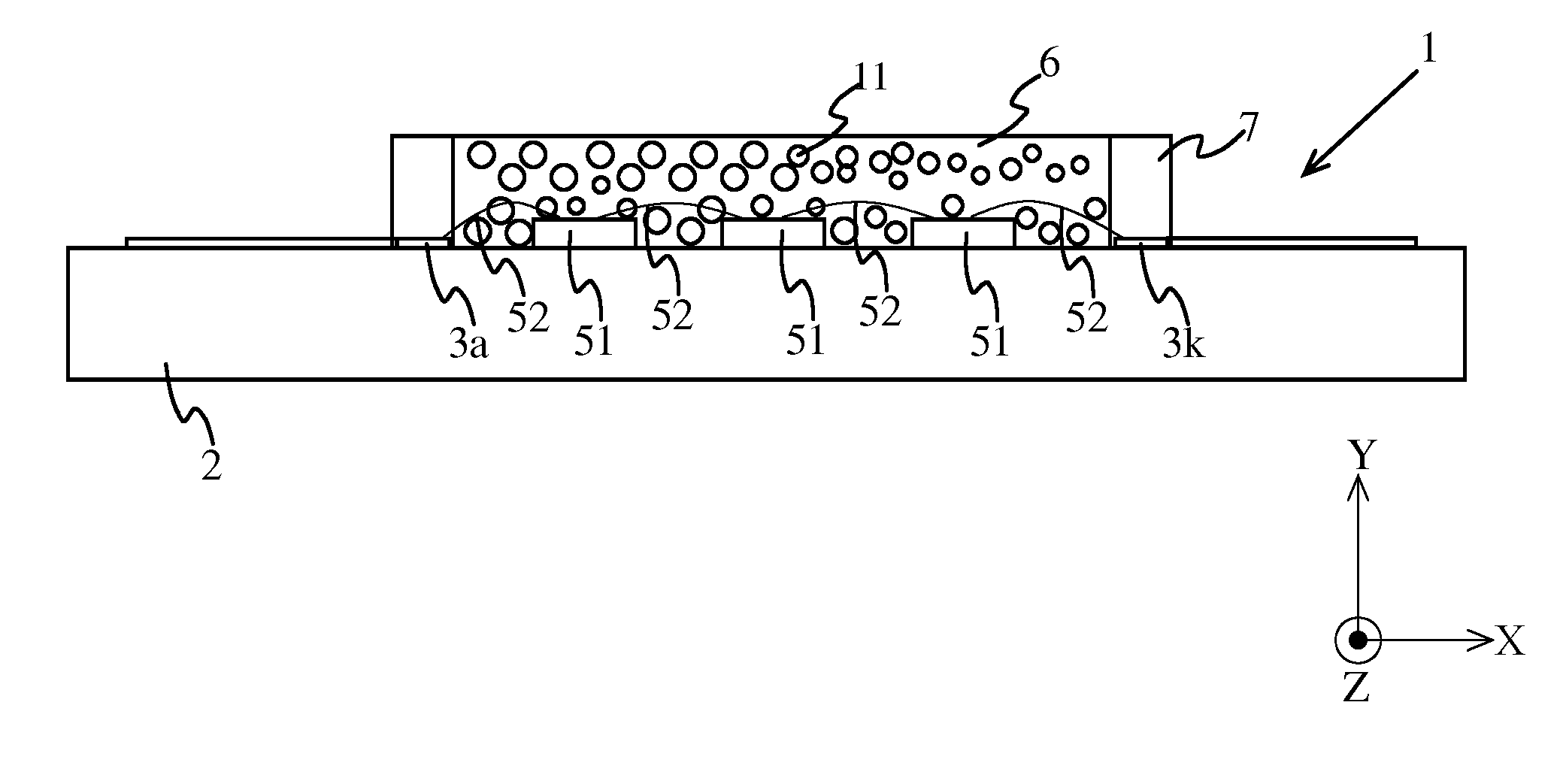
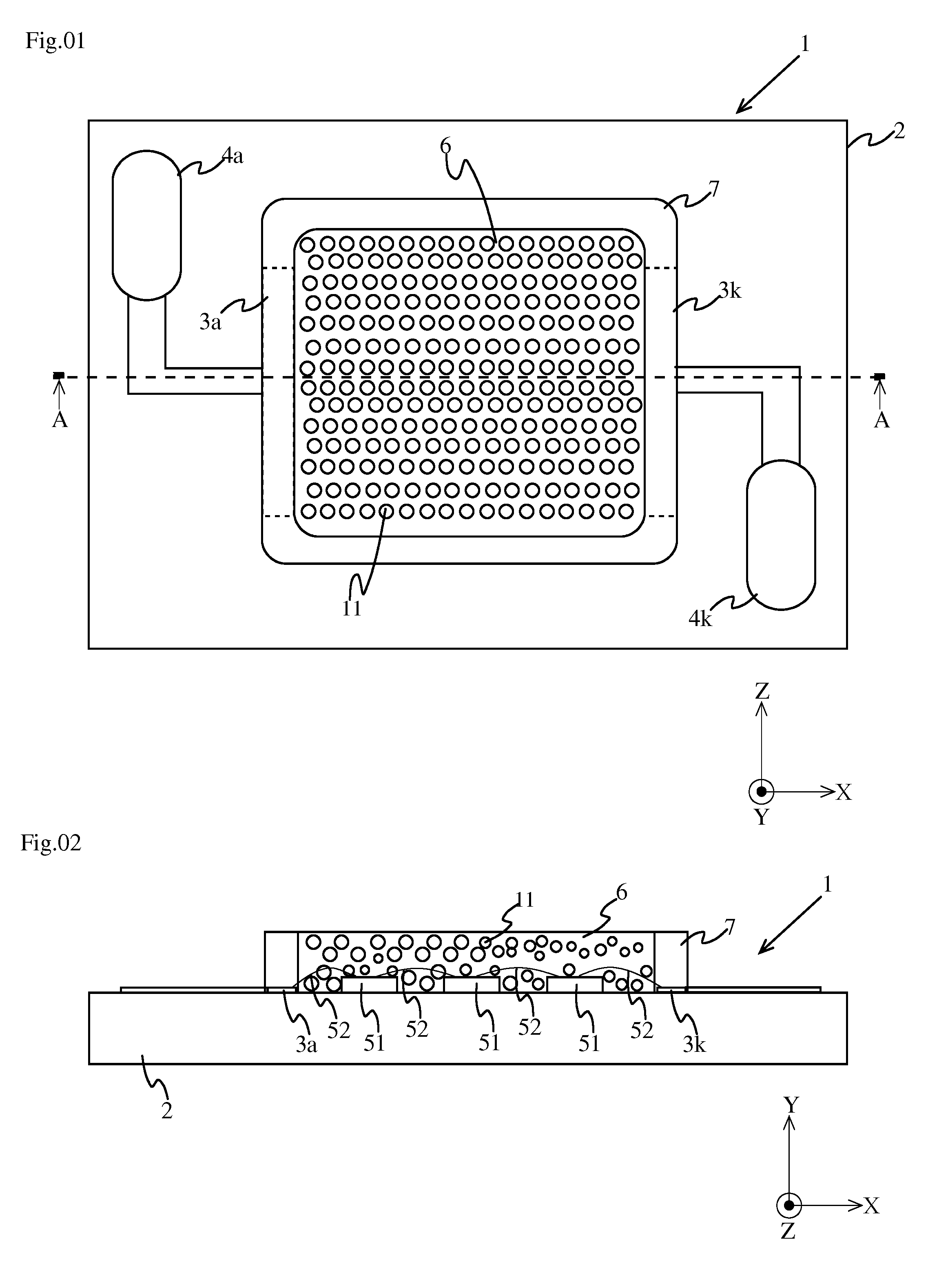
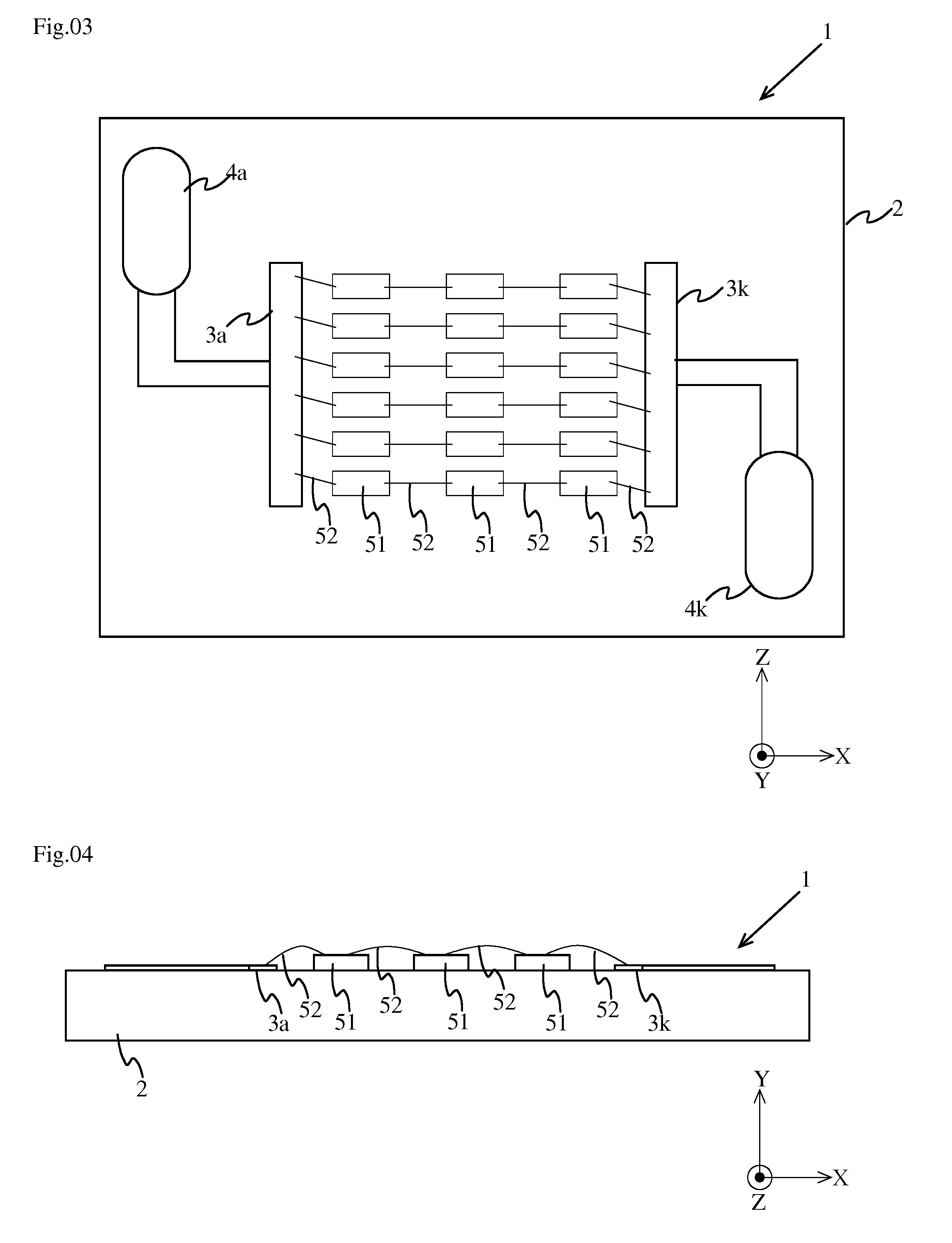
[0067]FIG. 5 is a top view of a light emitting device according to a second embodiment of the present invention. FIG. 6 is a side sectional view of the light emitting element shown in FIG. 5, taken on a YX section across line A-A. Here, the LED mounted on the substrate is similar to that in the first embodiment, and is therefore omitted from illustration. For such parts as find their counterparts in the first embodiment, no overlapping description will be repeated unless it is necessary.

[0068]The phosphor layer 6 is a resin layer which fills inside the resin frame 7 so as to cover the LED 5. The phosphor layer 6 emits light having a peak wavelength in a predetermined wavelength range by excitation with light (excitation light) emitted from the LED 5. The phosphor layer 6 is composed of a first phosphor layer 61 and a second phosphor layer 62. The first phosphor layer 61 is formed of sealing resin, which comprises silicone resin, containing a first phosphor 10 (indicated by triangula...

third embodiment

[0084]FIG. 7 is a top view showing a light emitting device according to a third embodiment of the present invention. FIG. 8 is a side sectional view of the light emitting device shown in FIG. 7, taken on an XY section across line B-B. FIG. 9 is a top view showing LEDs mounted on a substrate in the third embodiment. FIG. 10 is a schematic diagram showing a positional relationship between phosphor layers and LEDs. In FIG. 10, for an easy grasp of the positional relationship between phosphor layers and LEDs, triangular and circular symbols indicating the first and second phosphors 10 and 11, respectively, are omitted.

[0085]In the second embodiment described previously, the absorption of red light by the second phosphor layer 62 is reduced by stacking the first phosphor layer 61 over the second phosphor layer 62. In this embodiment, the absorption of red light by the second phosphor layer 62 is reduced without stacking the first and second phosphor layers together.

[0086]In this embodime...


PUM


Abstract

This light emitting device is provided with: a light emitting element which emits excitation light; and a far-red phosphor which is excited by the light of the light emitting element and emits light that has a peak wavelength within the range of 700-800 nm. The far-red phosphor has a median diameter within the range of 1-20 μm.

Description

TECHNICAL FIELD[0001]The present invention relates to light emitting devices.BACKGROUND ART[0002]The production and supply of plants such as vegetables and fruits are susceptible to drops due to climatic changes, pest damage, etc. On the other hand, today, with much attention paid to safe foods and higher food self-sufficiency, stable supply of safe plants is sought. This has brought about the development of technology for growing plants on factory equipment without using sunlight.[0003]To grow a plant on factory equipment (in a plant factory), light (a source of light) is needed as a substitute for sunlight. Nowadays, light emitting elements such as LEDs (light-emitting diodes) are used as light sources in lighting devices for plant growth.[0004]As is generally known, for efficient growth of plants in a plant factory, light having peak wavelengths in a plurality of wavelength regions is effective (peak wavelength denoting a wavelength at which a maximum relative radiation intensity...

Claims


Application Information

Patent Timeline
Patent Type & Authority Applications(United States)
IPC IPC(8): H01L33/50
CPCH01L33/504H01L33/508A01G7/045C09K11/7708H01L33/502H01L25/0753H01L2224/48137H01L2224/48091C09K11/77348H01L2924/00014Y02P60/14
Inventor ONUMA, HIROAKIMASUDA, MASATSUGUHATA, TOSHIO
Owner SHARP KK
Why Eureka
Try Eureka