Crystallization apparatus, crystallization method, and phase modulation device

a crystallization method and crystallization method technology, applied in the direction of polycrystalline material growth, electronic commutators, gel state, etc., can solve the problem of easy end of crystal growth midway, crystal growth is easy to end midway, and the design cannot be analytically performed with a prospect, etc. problem, to achieve the effect of large grain diameter and sufficient crystal growth

Inactive Publication Date: 2006-02-09
SHARP KK
View PDF3 Cites 15 Cited by
  • Summary
  • Abstract
  • Description
  • Claims
  • Application Information

AI Technical Summary

Benefits of technology

[0014] The present invention has been developed in view of the above-described problem of the conventional technique. An object of the present invention is to provide a crystallization apparatus and a crystallization method capable of realizing sufficient crystal growth from a crystal nucleus in a lateral direction and producing a crystallized semiconductor film having a large grain diameter.

Problems solved by technology

However, in the case where a large number of thin-film transistors are formed in the poly-silicon layer, fluctuations of crystal grain boundary number in a channel portion raise a problem.
However, since the light intensity does not increase linearly, growth of the crystals easily end midway.
Since a surplus irregularity distribution is easily generated in the periphery of the light intensity distribution having the inverse peak pattern, the light intensity distribution having the inverse peak pattern cannot be arranged into an array, or crystal grains cannot be generated in the array.
However, the design cannot be analytically performed with a prospect.
Even if the analytic design can be realized, it is expected that considerably complicated conditions are obtained.
However, it is difficult to grow the crystals having large grain diameters in the lateral direction.
It is generally difficult to form a film having a light absorption distribution which continuously changes.
Especially, when a film to be crystallized is irradiated with light having a very high intensity for the crystallization, deterioration of film materials of the film having the light absorption distribution is unfavorably easily caused by thermal or chemical changes by light absorption.

Method used


Image

  • Crystallization apparatus, crystallization method, and phase modulation device
  • Crystallization apparatus, crystallization method, and phase modulation device
  • Crystallization apparatus, crystallization method, and phase modulation device

Examples


embodiment 1

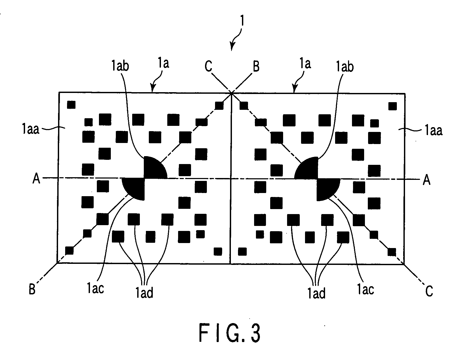
[0207]FIG. 3 is a diagram schematically showing a constitution of a phase modulation device according to Embodiment 1 of the present invention. The phase modulation device 1 is a phase modulation device for preparing a semiconductor thin film comprising a 5 μm square crystal grain array. The phase modulation device 1 comprises a plurality of unit areas 1a having the same pattern, and the respective unit areas 1a are two-dimensionally arranged in a predetermined period. In FIG. 3, for simplicity of description, only two adjacent unit areas 1a having square shapes are shown. One side of each of the unit areas 1a is 5 μm in accordance with a converted value in the image plane of the optical image forming system 4. Dimensions of the phase modulation device 1 will be described hereinafter in accordance with converted values in the image plane of the optical image forming system 4.

[0208] The unit area 1a comprises a reference face (blank portion in the drawing) 1aa having a certain phase...

embodiment 2

[0252]FIG. 16 is a diagram schematically showing a constitution of the phase modulation device in Embodiment 2 of the present invention. A phase modulation device 1 is a phase modulation device for preparing a semiconductor thin film comprising a 5 μm square crystal grain array in the same manner as in Embodiment 1, and has a constitution similar to that of Embodiment 1. However, in Embodiment 2, a first area 1ab, a second area 1ac, and all third areas 1ad have a phase of −90° (+90° in Embodiment 1) with respect to a reference face 1aa. Embodiment 2 is different from Embodiment 1 in this respect. Embodiment 2 will be hereinafter described noting a difference from Embodiment 1.

[0253] In Embodiment 2, on the surface of a substrate 5 to be treated, defocused in a direction (lower part of FIG. 1) distant from an optical image forming system 4 by 5 μm (i.e., defocus of −5 μm) from a calculated focus position of the optical image forming system 4 and positioned, a light intensity distrib...

embodiment 3

[0259]FIG. 19 is a diagram schematically showing a constitution of a phase modulation device according to Embodiment 3 of the present invention. A phase modulation device 1 is a phase modulation device for preparing a semiconductor thin film comprising a 5 μm square crystal grain array in the same manner as in Embodiments 1 and 2, and has a constitution similar to that of Embodiment 1. However, in Embodiment 3, eight 0.2 μm square third areas 1ae having square shapes are arranged around a first area 1ab and a second area 1ac, and the first area 1ab, the second area 1ac, and all the third areas 1ae have a phase of +100° (+90° in Embodiment 1) with respect to a reference face 1aa. Embodiment 3 is different from Embodiment 1 in this respect. Embodiment 3 will be hereinafter described noting a difference from Embodiment 1.

[0260] Although not shown, in Embodiment 3, a position defocused in a direction (lower part of FIG. 1) distant from an optical image forming system 4 by 7 μm (i.e., d...


PUM

PropertyMeasurementUnit
sizeaaaaaaaaaa
sizeaaaaaaaaaa
wavelengthaaaaaaaaaa

Abstract

A crystallization apparatus of the present invention irradiates a non-single-crystal semiconductor film with a luminous flux having a predetermined light intensity distribution to crystallize the film, and comprises a phase modulation device comprising a plurality of unit areas which are arranged in a certain period and which mutually have substantially the same pattern, and an optical image forming system disposed between the phase modulation device and the non-single-crystal semiconductor film. The unit area of the phase modulation device has a reference face having a certain phase, a first area disposed in the vicinity of a center of each unit area and having a first phase difference with respect to the reference face, and a second area disposed in the vicinity of the first area and having substantially the same phase difference as that of the first phase difference with respect to the reference face.

Description

CROSS-REFERENCE TO RELATED APPLICATIONS [0001] This application is based upon and claims the benefit of priority from prior Japanese Patent Applications No. 2004-226668, filed Aug. 3, 2004; and No. 2004-226669, filed Aug. 3, 2004, the entire contents of both of which are incorporated herein by reference. BACKGROUND OF THE INVENTION [0002] 1. Field of the Invention [0003] The present invention relates to a crystallization apparatus, a crystallization method, and a phase modulation device, particularly to a crystallization apparatus which irradiates a polycrystal or amorphous semiconductor film with laser light having a predetermined light intensity distribution to produce a crystallized semiconductor film. [0004] 2. Description of the Related Art [0005] A thin-film transistor (TFT), for example, for use in a switching device which controls a potential applied to a pixel of a liquid crystal display (LCD) has heretofore been formed in an amorphous silicon layer or a poly-silicon layer....

Claims


Application Information

Patent Timeline
Patent Type & Authority Applications(United States)
IPC IPC(8): C30B23/00C30B25/00C30B28/12C30B28/14
CPCC30B1/00Y10T117/1004C30B13/24H02P6/08H02P6/16
Inventor KATO, TOMOYAMATSUMURA, MASAKIYOTANIGUCHI, YUKIO
Owner SHARP KK
Why Eureka
Try Eureka