Crystallization apparatus, crystallization method, device and phase modulation element

a crystallization apparatus and crystallization method technology, applied in the direction of separation processes, instruments, manufacturing tools, etc., can solve the problems of obstructing excellent crystallization, obstructing crystallization, and affecting crystallization efficiency, so as to achieve sufficient crystal growth

Inactive Publication Date: 2007-05-08
SHARP KK
View PDF2 Cites 12 Cited by
  • Summary
  • Abstract
  • Description
  • Claims
  • Application Information

AI Technical Summary

Benefits of technology

[0016]In view of the above-described drawbacks, it is an object of the present invention to provide a crystallization apparatus and a crystallization method which can obtain a light intensity distribution having a desired gradient for performing crystallization with a large grain size, and can realize a sufficient crystal growth in a lateral direction from a crystal nucleus, thereby crystallizing a non-crystal semiconductor film with a large grain size.

Problems solved by technology

Additionally, many thin film transistors formed on the polycrystal silicon have a problem of irregularities in crystal grain boundary number in a channel portion.
Moreover, in regard to application of a laser beam with the mask 1 and mask 2 being in close vicinity to the substrate, an operation which always maintains a distance of several μm order between the mask #1 and the substrate constant requires a long time, thereby relatively delaying a tact time.
However, in the conventional technique (proximity method) by which a substrate is in close proximity to an element, the element is contaminated due to ablation in a semiconductor film, which obstructs the excellent crystallization.
Additionally, the substrate and the element must be separated from each other every time processing moves to another processing area on the substrate, which prolongs the processing time.
Further, since a gap which should be set between the element and the substrate is very small, a detection light beam for position detection is hard to be led into this narrow light path, and a gap adjustment is difficult.
On the other hand, in the conventional technique using a phase shifter having a line-and-space pattern whose phase difference is 180 degrees, a trough portion in a formed light intensity distribution with an inverse peak pattern becomes too deep.
In this case, since a crystal does not grow unless a light intensity is not less than a predetermined threshold value, an uncrystallized area becomes too large, and a crystallized semiconductor film with a large grain size cannot be generated.
Furthermore, it is impossible to obtain a large gradient of a light intensity distribution pattern with an inverse peak pattern in order to perform crystallization with a large grain size.

Method used


Image

  • Crystallization apparatus, crystallization method, device and phase modulation element
  • Crystallization apparatus, crystallization method, device and phase modulation element
  • Crystallization apparatus, crystallization method, device and phase modulation element

Examples


Embodiment Construction

[0073]Embodiments according to the present invention will now be described with reference to the accompanying drawings.

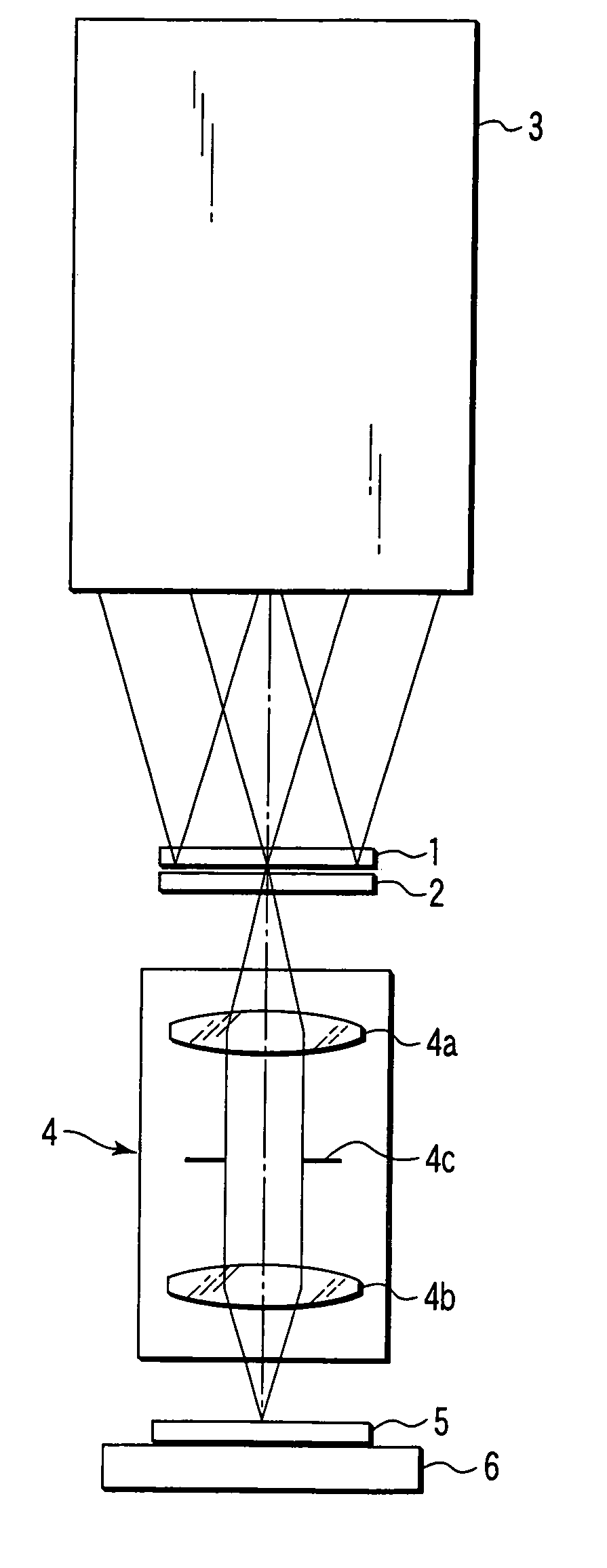
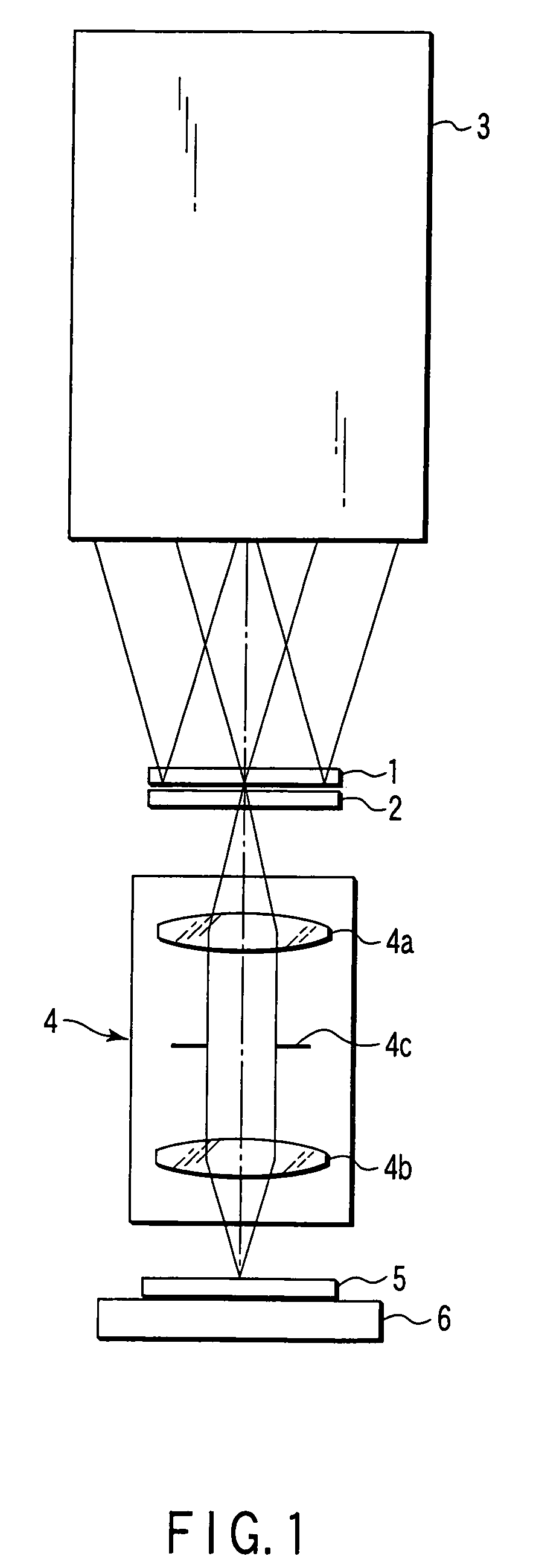
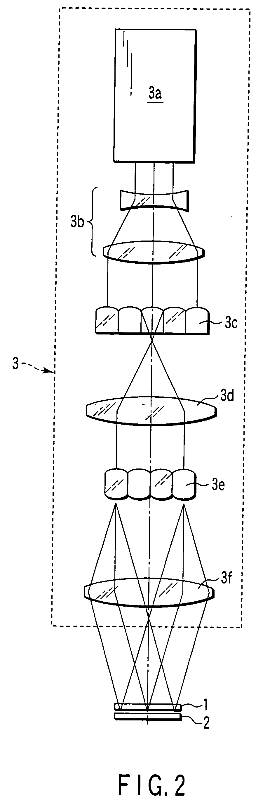
[0074]FIG. 1 is a view schematically showing a structure of a crystallization apparatus according to a first embodiment of the present invention. Further, FIG. 2 is a view schematically showing an internal structure of an illumination system of FIG. 1. A description will be given with reference to FIGS. 1 and 2. A crystallization apparatus according to the first embodiment comprises a first phase modulation element 1 which forms an optical pattern having a desired light intensity gradient distribution to incident light beam, and a second phase modulation element 2 having a pattern which forms a light intensity minimum distribution with an inverse peak shape. Structures of the first phase modulation element 1 and the second phase modulation element 2 will be described later.

[0075]It is to be noted that the first phase modulation element 1 and the second phase modulat...


PUM

PropertyMeasurementUnit
wavelengthaaaaaaaaaa
area share ratiosaaaaaaaaaa
thicknessaaaaaaaaaa

Abstract

The present invention comprises a light modulation optical system having a first element which forms a desired light intensity gradient distribution to an incident light beam and a second element which forms a desired light intensity minimum distribution with an inverse peak shape to the same, and an image formation optical system which is provided between the light modulation optical system and a substrate having a polycrystal semiconductor film or an amorphous semiconductor film, wherein the incident light beam to which the light intensity gradient distribution and the light intensity minimum distribution are formed is applied to the polycrystal semiconductor film or the amorphous semiconductor film through the image formation optical system, thereby crystallizing a non-crystal semiconductor film. The pattern of the first element is opposed to the pattern of the second element.

Description

CROSS-REFERENCE TO RELATED APPLICATIONS[0001]This application is based upon and claims the benefit of priority from the prior Japanese Patent Application No. 2003-339363, filed Sep. 30, 2003, the entire contents of which are incorporated herein by reference.BACKGROUND OF THE INVENTION[0002]1. Field of the Invention[0003]The present invention relates to a crystallization apparatus which crystallizes a non-crystal semiconductor film with irradiating laser beam to a film made of polycrystal semiconductor or an amorphous semiconductor, a phase modulation element used in this crystallization apparatus, a crystallization method, and a device. In particular, the present invention relates to a crystallization apparatus which crystallizes a non-crystal semiconductor film, such as a polycrystal semiconductor or an amorphous semiconductor, with irradiating laser beam having a predetermined light intensity distribution subjected to phase modulation by using a phase modulation element to a film ...

Claims


Application Information

Patent Timeline
Patent Type & Authority Patents(United States)
IPC IPC(8): C30B35/00H01L21/324B01D9/00B23K26/073C30B1/00C30B13/24G02B27/09G02F1/00G02F1/136H01L21/00H01L21/20H01L21/36
CPCB23K26/073C30B13/24G02B27/0927G02B27/0961Y10T117/10Y10S117/90Y10T117/1004Y10T117/1008H01L21/2026H01L21/02686H01L21/02691H01L21/02488H01L21/02422H01L21/02678H01L21/02532H01L21/324H01L21/0268H01L21/02595
Inventor TANIGUCHI, YUKIOMATSUMURA, MASAKIYOAKITA, NORITAKA
Owner SHARP KK
Why Eureka
Try Eureka