

Systems and methods for plasma filtering
Patent Information
- Authority / Receiving Office
- CN · China
- Patent Type
- Applications(China)
- Current Assignee / Owner
- APPLIED MATERIALS INC
- Publication Date
- 2019-12-13
Smart Images
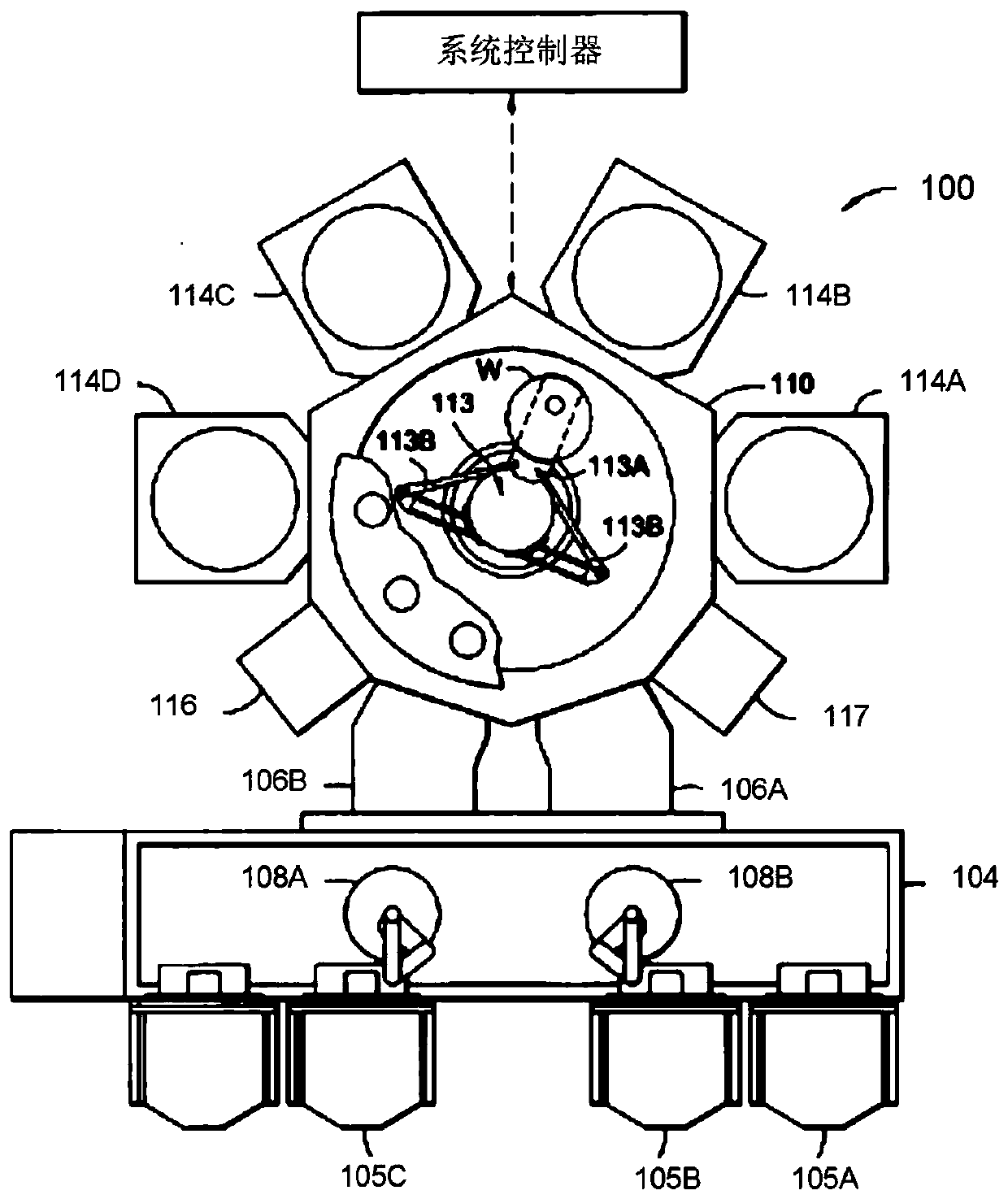
Figure 1 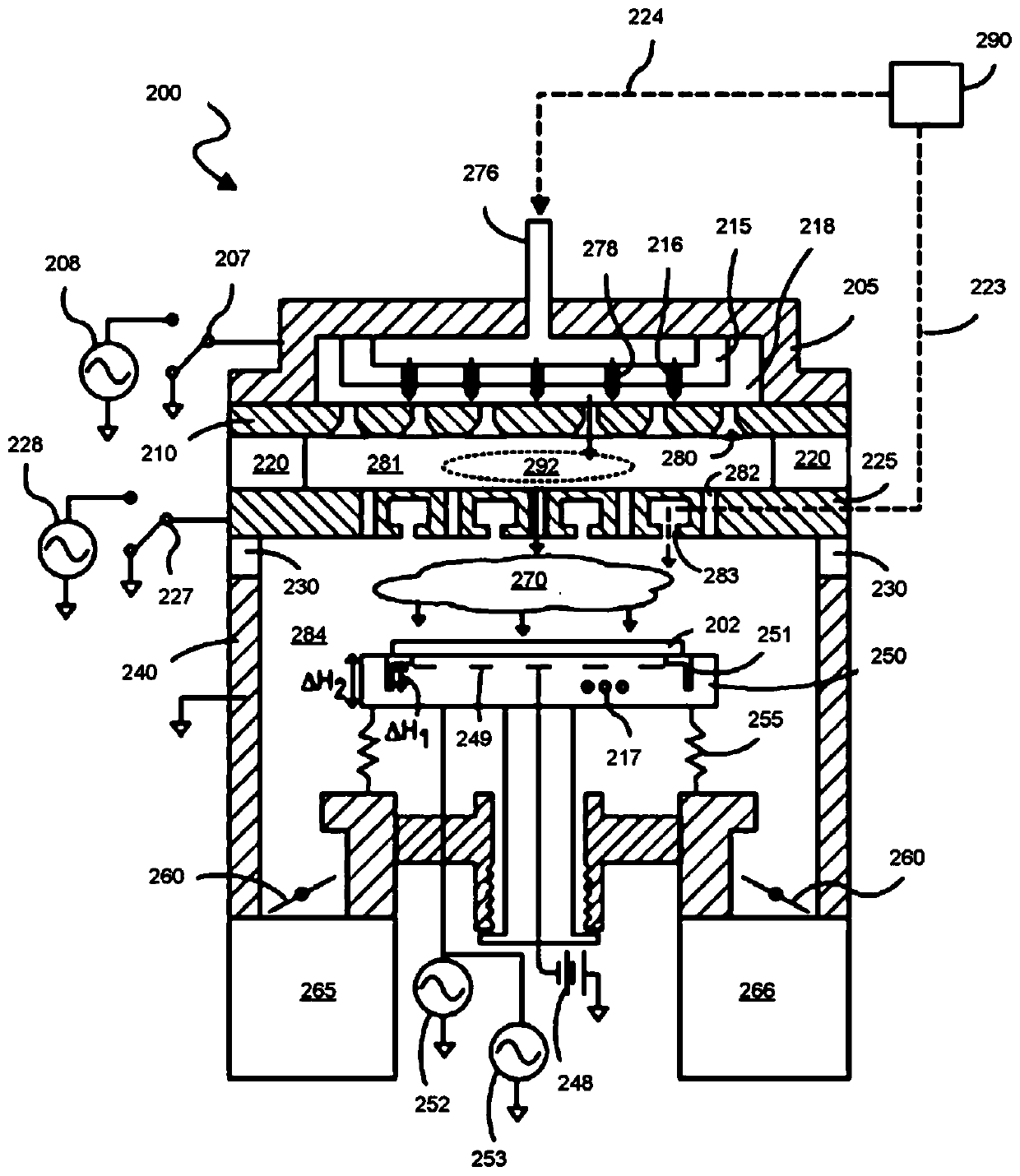
Figure 2 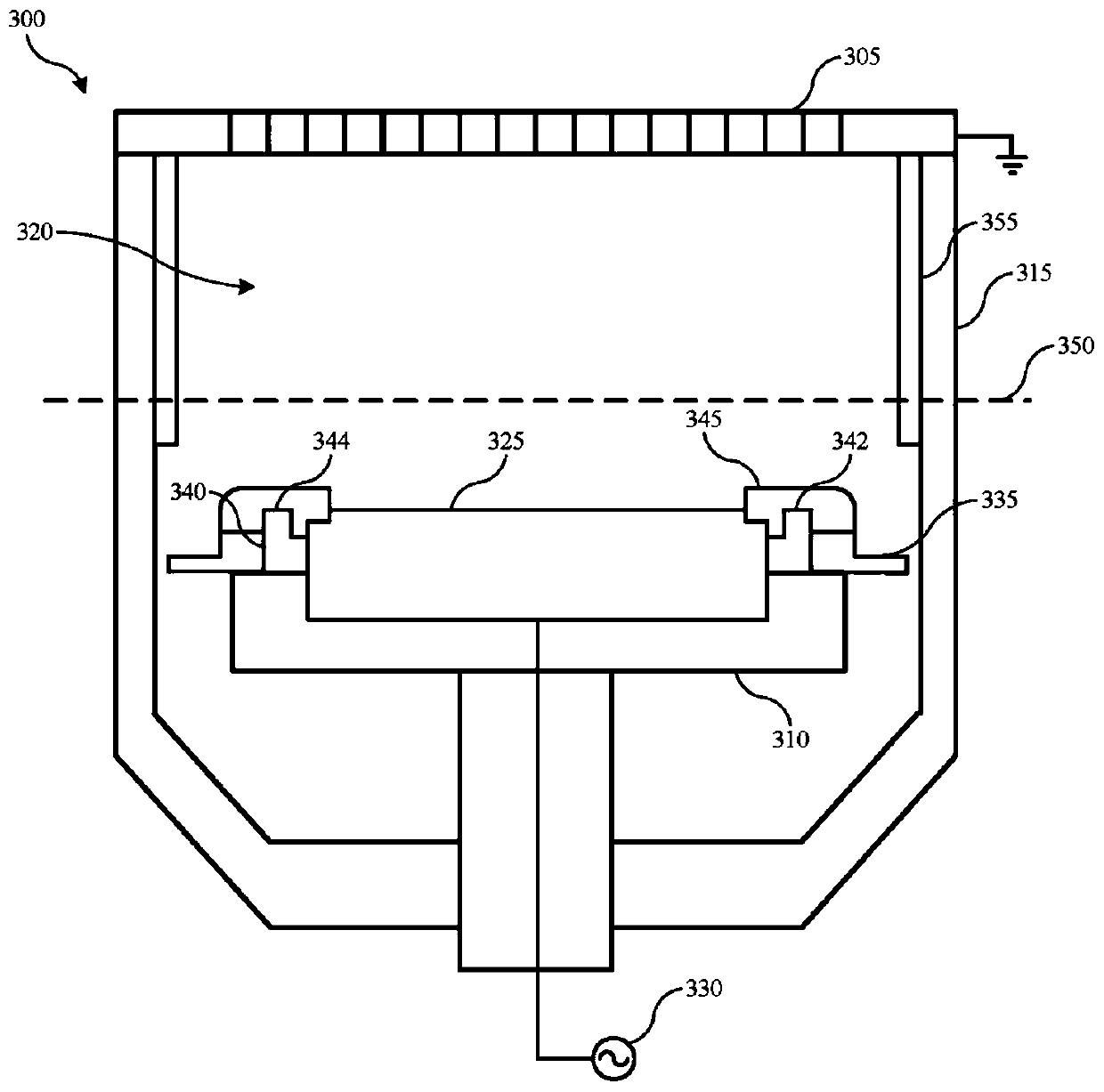
Figure 3
Abstract
Description
[0001] This application is a divisional application of a Chinese patent application with the filing date of October 24, 2018, the application number 201811245601.3, and the title "System and Method for Plasma Filtration". technical field
[0002] The technology relates to semiconductor systems, methods and devices. More specifically, the present technology relates to systems and methods for filtering plasma within processing chambers. Background technique
[0003] Integrated circuits may be fabricated by processes that produce intricately patterned layers of material on the surface of a substrate. Generating patterned material on a substrate requires a controlled method for removing exposed material. Chemical etching is used for a variety of purposes, including transferring the pattern in the photoresist to underlying layers, thinning layers, or thinning the lateral dimensions of features already present on the surface. It is often desirable to have an etch process that et...