Novel display panel surface defect detection system

A display panel and defect detection technology, which is applied in the direction of optical testing defect/defect, measuring device, optics, etc., can solve problems such as damage to the supporting structure of the pixel display area, poor display of the display panel, scratches on the surface of the display panel, etc., to improve the equipment Marriage rate, reduced equipment maintenance costs, stable and reliable adsorption effect

Inactive Publication Date: 2020-02-28
周娇
View PDF4 Cites 4 Cited by
  • Summary
  • Abstract
  • Description
  • Claims
  • Application Information

AI Technical Summary

Problems solved by technology

[0002] Most of the existing small and medium-sized display panels are liquid crystal LCD, OLED, etc. Due to the complexity of product structure and production process, some visual defects will inevitably appear in the manufacturing process
For example, in the manufacturing process of display panels, transportation is a basic technical link. However, with the increasingly high requirements for ultra-thin and touch touch, the existing transportation technology has more and more exposed the following problems: when When transported by a suction cup, the debris attached to the suction cup will often scratch the surface of the display panel, and the pressure of the suction cup will easily damage the support structure of the pixel display area, resulting in poor display of the display panel
[0005] The above-mentioned display panel surface defect detection system based on machine vision mainly has the following shortcomings: when the image processing unit analyzes and processes the panel pictures collected by the image acquisition unit, since the panel pictures often include surface scratches, pits, Damage and other real bad defects, as well as erasable surface foreign objects such as surface dust and dirt, so the image processing unit often needs to use very complex algorithms to distinguish between real bad defects and surface foreign objects, which has complex image processing processes and consumes a lot of time. The question of duration

Method used


Image

  • Novel display panel surface defect detection system
  • Novel display panel surface defect detection system
  • Novel display panel surface defect detection system

Examples


Embodiment 1

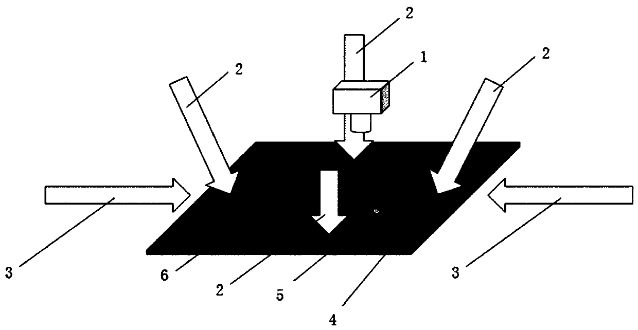
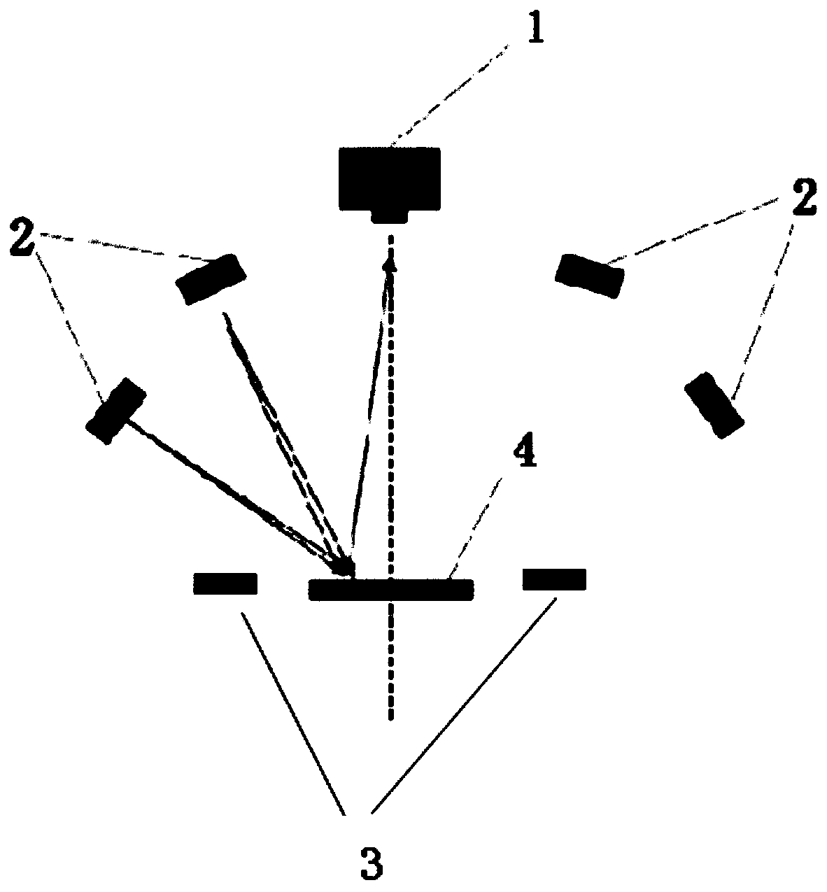
[0084] Turn on the main light source and the auxiliary light source to take pictures in time-sharing, that is: only the main optical unit is turned on, and when the auxiliary optical unit is not turned on, the image acquisition device collects the image of the detected display panel, which is recorded as the first original detection image; only the auxiliary optical unit is turned on , when the main optical unit is not turned on, the image acquisition device acquires the image of the detected display panel, which is recorded as the second original detection image; the image acquisition device uploads both the first original detection image and the second original detection image to the image processing unit;

[0085] The image processing unit compares and analyzes the first original detection image and the second original detection image, and based on the second original detection image, eliminates the erasable foreign matter on the surface from the first original detection imag...

Embodiment 2

[0087] Turn on the main light source and auxiliary light source at the same time, but choose different light source colors for the main light source and auxiliary light source. The preferred color combination of the main light source and the auxiliary light source may be the mode of "blue+red" or "red+blue". Then use the image acquisition device to collect the image of the detected display panel, which is recorded as the third original detection image; and upload the third original detection image to the image processing unit;

[0088] The image processing unit analyzes the third original detection image according to the color characteristics. Since the auxiliary light source can illuminate dust and other surface erasable foreign objects but cannot illuminate real bad defects, the main light source can illuminate real bad defects and surface erasable foreign objects. The foreign matter is illuminated at the same time. Therefore, the image processing unit can distinguish the re...


PUM

PropertyMeasurementUnit
diameteraaaaaaaaaa

Abstract

The invention provides a novel display panel surface defect detection system. A defect identification subsystem comprises an image acquisition device, a main optical unit, an auxiliary optical unit and an image processing unit. The image acquisition device is connected with the image processing unit; and the system further comprises a reversible double-sided adsorption device and a light source brightness self-adaptive adjustment system. The system has the advantages that: (1) in the bad identification subsystem, the image processing unit can simply and quickly distinguish real bad defects andsurface foreign matters in a picture, and the system has the advantages of the simple image processing process, the high speed and the high efficiency; (2) in the reversible double-sided adsorption device, a panel is adsorbed from a bottom surface, the adsorption is stable and reliable, and the machine vision photographing is not influenced; and the double-sided adsorption structure can rotate the panel by 180 degrees and can stably adsorb the panel again; and (3) the light source brightness self-adaptive adjustment system can greatly prolong the service life of the light source, can improvethe activation rate of the device and can effectively reduce the maintenance cost of the device.

Description

technical field [0001] The invention belongs to the technical field of display panel defect detection, and in particular relates to a novel display panel surface defect detection system. Background technique [0002] Most of the existing small and medium-sized display panels are liquid crystal LCD, OLED, etc. Due to the complexity of product structure and production process, some visual defects inevitably appear in the manufacturing process. For example, in the manufacturing process of display panels, transportation is a basic technical link. However, with the increasingly high requirements for ultra-thin and touch touch, the existing transportation technology has more and more exposed the following problems: when When transported by a suction cup, the debris attached to the suction cup will often scratch the surface of the display panel, and the pressure of the suction cup will easily damage the support structure of the pixel display area, resulting in poor display of the d...

Claims


Application Information

Patent Timeline
Patent Type & Authority Applications(China)
IPC IPC(8): G01N21/95G01N21/94G01N21/88G02F1/13B25H1/10
CPCG01N21/95G01N2021/9513G01N21/94G01N21/8806G01N21/8851G02F1/1309B25H1/10G01N2021/8854G01N2021/8887
Inventor 何祥飞肖丽那
Owner 周娇
Why Eureka
Try Eureka