Blue light device with high efficiency and long service life

A long-life, blue-light technology, applied in the direction of electric solid-state devices, semiconductor devices, semiconductor/solid-state device manufacturing, etc., can solve the problems of reducing the efficiency and life of blue-light devices, blue phosphorescent devices cannot meet practical applications, etc., and achieve low working voltage , high efficiency effect

Active Publication Date: 2020-10-02
SHANGHAI CHUANQIN NEW MATERIAL CO LTD
View PDF11 Cites 3 Cited by
  • Summary
  • Abstract
  • Description
  • Claims
  • Application Information

AI Technical Summary

Problems solved by technology

However, due to the high energy gap of blue light, there are great problems in the stability and optical purity of blue phosphorescent materials, and blue phosphorescent devices cannot meet practical applications, making the current blue light devices still based on blue fluorescent materials, which will cause blue Devices require higher voltage and current density, which reduces the efficiency and lifetime of blue light devices, so it is necessary to develop high-efficiency and long-life blue light devices

Method used


Image

  • Blue light device with high efficiency and long service life
  • Blue light device with high efficiency and long service life
  • Blue light device with high efficiency and long service life

Examples


Embodiment 1

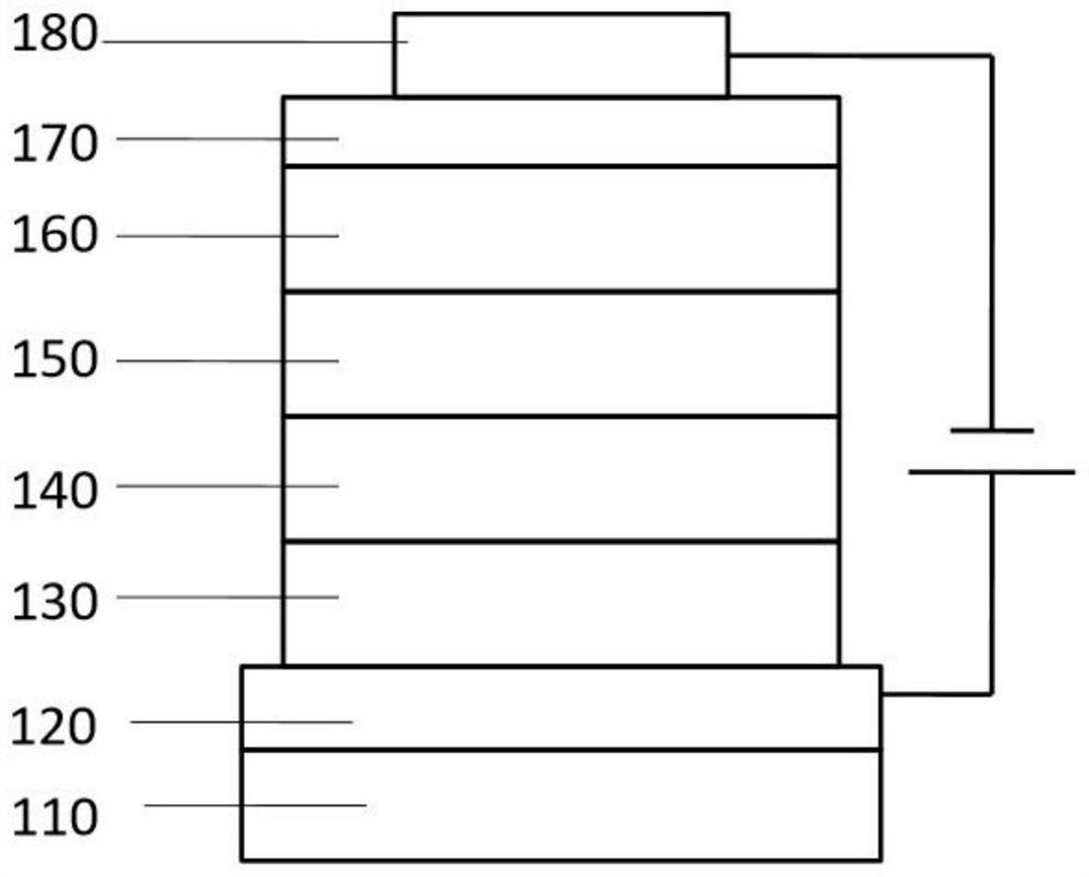
[0057] First, the transparent conductive ITO glass substrate 110 (with the anode 120 on it) (CSG Group Co., Ltd.) was washed with deionized water, ethanol, acetone, and deionized water in sequence, and then treated with oxygen plasma for 30 seconds. Next, a 5 nm thick HIL was evaporated on the anode 120 as the hole injection layer 130; the compound HTL was continuously evaporated to form a 70 nm thick hole transport layer 140. Then, a 25-nm-thick light-emitting layer 150 was vapor-deposited on the hole transport layer, in which BH6 was the host light-emitting material, and 3% by weight of BD6 was used as the guest material. Then, an electron transport layer 160 with a thickness of 25 nm is vapor-deposited on the light-emitting layer, wherein the ratio of ET2 and LiQ is 50:50. Finally, vapor deposition of 1 nm LiF as the electron injection layer 170 and 100 nm Al as the device cathode 180.

[0058] The prepared device uses Photo Research PR650 spectrometer at 10mA / cm 2 The test w...

Embodiment 2

[0060] The difference from Example 1 is that the guest material in the light-emitting layer uses BD8 instead of BD6, and the electron transport material uses ET6 instead of ET2.

Embodiment 3

[0062] The difference from Example 1 is that the host material in the light-emitting layer uses BH9 instead of BH6, and the electron transport material uses ET6 instead of ET2.


PUM

PropertyMeasurementUnit
thicknessaaaaaaaaaa
thicknessaaaaaaaaaa
thicknessaaaaaaaaaa

Abstract

The invention belongs to the technical field of organic light-emitting device display, and particularly relates to a blue light device with high efficiency and long service life. The blue light devicecomprises an anode, a cathode and an organic layer, the organic layer comprises more than one blue light emitting layer and more than one electron transport layer, and the light-emitting layer is used in combination with the electron transport layer. The blue light emitting layer is composed of a host material represented by the following formula 1 and an object material represented by the following formula 2, and the electron transport layer is prepared from the co-evaporation of a compound represented by a formula 3 and an organic alkali metal compound.

Description

Technical field: [0001] The invention belongs to the field of organic electroluminescent device display technology, and more specifically, relates to a blue light device with high efficiency and long life. Background technique: [0002] Organic electroluminescent devices (OLEDs), as a new type of display technology, have self-luminous, wide viewing angle, low energy consumption, high efficiency, thinness, rich colors, fast response speed, wide applicable temperature range, low driving voltage, and flexible manufacturing The flexible and transparent display panel and its unique advantages such as environmental friendliness can be applied to flat panel displays and new-generation lighting, and can also be used as LCD backlights. [0003] An organic electroluminescent device is a device prepared by depositing a layer of organic material between two metal electrodes by spin coating or vacuum evaporation. A classic three-layer organic electroluminescent device includes a hole transport ...

Claims


Application Information

Patent Timeline
Patent Type & Authority Applications(China)
IPC IPC(8): H01L51/50H01L51/54
CPCH10K85/615H10K85/622H10K85/631H10K85/626H10K85/636H10K85/633H10K85/654H10K85/6574H10K50/11H10K50/16
Inventor 苏艳宋文轩周海涛黄珠菊
Owner SHANGHAI CHUANQIN NEW MATERIAL CO LTD
Why Eureka
Try Eureka