

A magnetic field testing device for semiconductor current density inversion
A technology of current density and testing equipment, which is applied in the field of power semiconductor device testing, and can solve problems such as difficult detection of current density distribution
- Summary
- Abstract
- Description
- Claims
- Application Information
AI Technical Summary
Problems solved by technology
Method used
Image

Examples
Embodiment Construction
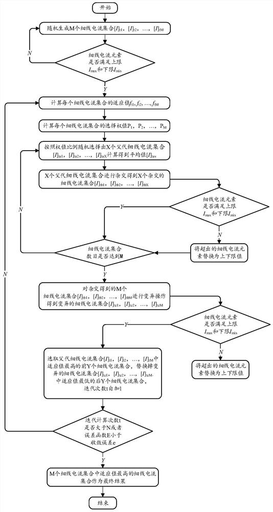
[0062] The technical solutions of the present invention will be clearly and completely described below with reference to the embodiments of the present invention. Obviously, the described embodiments are only a part of the embodiments of the present invention, rather than all the embodiments. Based on the embodiments of the present invention, all other embodiments obtained by those of ordinary skill in the art without creative efforts shall fall within the protection scope of the present invention.
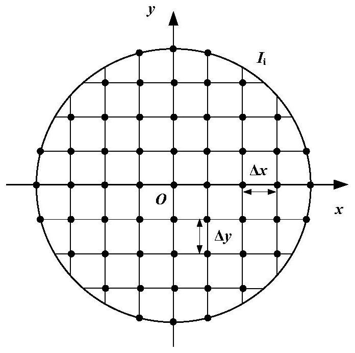
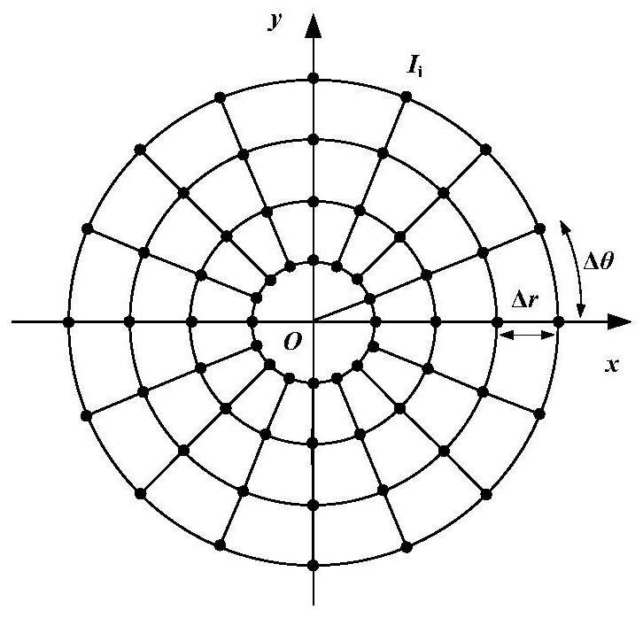
[0063]This embodiment integrates the magnetic field testing device into the magnetic field inversion current calculation method for semiconductor current density analysis. The theoretical basis is: when the cylindrical conductor structure is flowing, if there is an uneven distribution of current density in a thin cylindrical layer, then the magnetic field component at the position of the coplanar concentric circle (such as the radial magnetic field component) will have obvious cha...
PUM
 Abstract
Description
Claims
Application Information