Flash memory device with stable source line regardless of bit line coupling and loading effect

A storage device and flash technology, applied in information storage, read-only memory, static memory, etc., can solve the problems of reduced storage unit characteristics and increased chip size

Inactive Publication Date: 2004-03-24
SAMSUNG ELECTRONICS CO LTD
View PDF0 Cites 15 Cited by
  • Summary
  • Abstract
  • Description
  • Claims
  • Application Information

AI Technical Summary

Problems solved by technology

[0010] However, the method of forming an additional discharge path, along with it, has the disadvantage of increasing the chip size
Likewise, the method of forming metal strips or transistors between arrays of memory cells, with shapes different from the pattern of the memory cells, is limited by degrading the characteristics of the memory cells due to loading effects that occur during fabrication at storage unit

Method used


Image

  • Flash memory device with stable source line regardless of bit line coupling and loading effect
  • Flash memory device with stable source line regardless of bit line coupling and loading effect
  • Flash memory device with stable source line regardless of bit line coupling and loading effect

Examples


Embodiment Construction

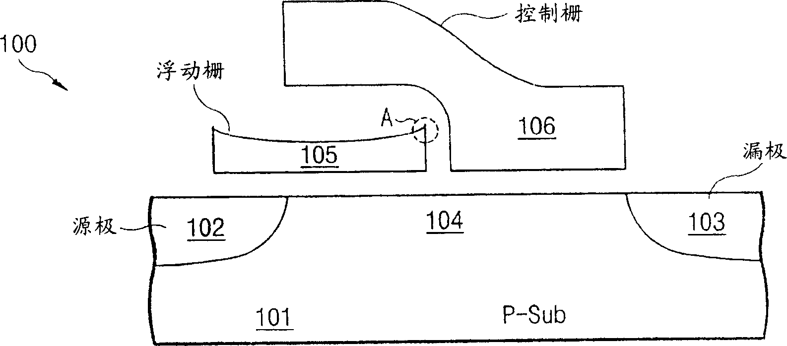
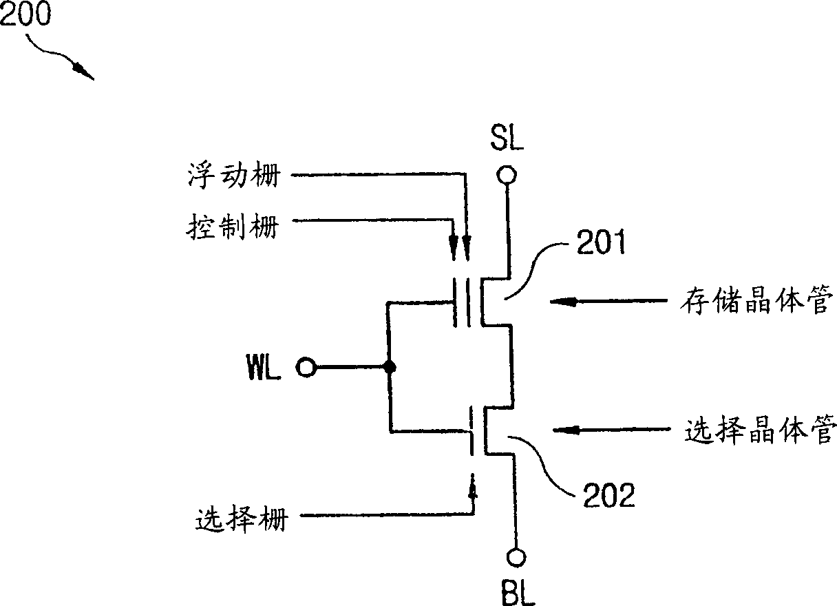
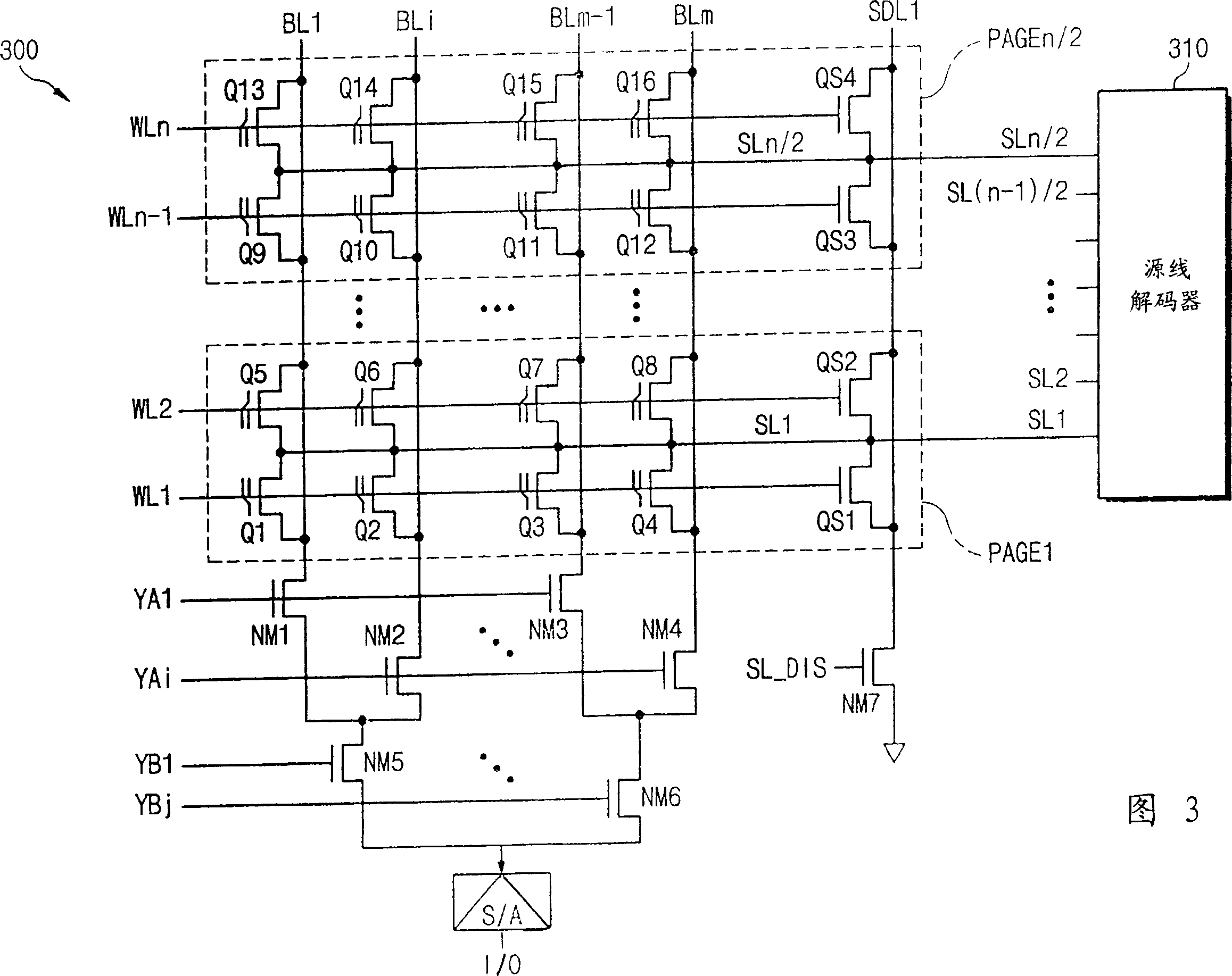
[0027] FIG. 5 is a schematic diagram of a flash memory device according to an embodiment of the present invention. Referring to FIG. 5, compared with the conventional memory cell array block 300 of FIG. 3, in the memory cell array block 300 of FIG. The cell array block 500 includes selection transistors QS51 to QS54 having the same structure as memory cell transistors Q1 to Q16. In other words, memory cell transistors Q1 to Q16 and selection transistors QS51 to QS54 are both in the form of split gate transistors as figure 1 type shown. Memory cell transistors Q1 to Q16 are "off" cells that can be selectively programmed, or "on" cells that are not programmed, while selection transistors QS51 to QS54 are "on" cells that are not programmed. In this structure, the source line discharge signal SL_DIS is inverted by the inverter INV1 and sent to the discharge line SDL1.

[0028] In this case, in the read and erase modes, a voltage of 0V is applied to the discharge line SDL1 servi...


PUM


Abstract

A flash memory device provides for a stable source line regardless of bit line coupling during a read operation and regardless of loading effect during a manufacturing process. The flash memory device includes: a plurality of flash memory cells arranged in rows and columns, each of the flash memory cells having a control gate, a source and a drain; a plurality of first, odd-numbered word lines each of which is connected with corresponding control gate of a first set of the flash memory cells; a plurality of second, even-numbered word lines each of which is connected with corresponding control gate of a second set of the flash memory cells; a plurality of bit lines each of which is connected with corresponding a drain of the flash memory cells; and a plurality of selection transistors connected between a source line and a discharge line, the source line being connected to sources of the first and second sets of flash memory cells, the selection transistors comprising the same structure as the first and second sets of the flash memory cells.

Description

technical field [0001] The present invention relates to a semiconductor memory device, and more particularly to a flash memory device with a stable source line, which does not take into account bit line coupling during a read operation, and does not take into account loading effects experienced during fabrication. Background technique [0002] Flash memory devices are widely used in computer and electronic communication systems that require storage capabilities. In flash memory devices, non-volatility and on-chip programmability are important factors for storing data in various applications. For example, for personal computers, flash memory devices are used to store BIOS boot information, or for portable devices such as mobile phones and digital cameras, flash memory devices are used to store program or data files. [0003] Unlike volatile memory such as Dynamic Random Access Memory (Dynamic Random Access Memory, DRAM), flash memory devices perform erase and program operati...

Claims


Application Information

Patent Timeline
Patent Type & Authority Applications(China)
IPC IPC(8): G11C16/00G11C16/04G11C16/08
CPCG11C16/0425G11C16/08G11C16/00
Inventor 郑晖泽
Owner SAMSUNG ELECTRONICS CO LTD
Why Eureka
Try Eureka