

Thin-film transistor including two-dimensional semiconductor and display apparatus including the same
a technology of thin-film transistors and display devices, applied in non-linear optics, identification means, instruments, etc., can solve the problems of increased manufacturing costs, low mobility and limited use of amorphous silicon thin-film transistors in active matrix organic light-emitting devices (amoleds). achieve excellent electrical properties
- Summary
- Abstract
- Description
- Claims
- Application Information
AI Technical Summary
Benefits of technology
Problems solved by technology
Method used
Image

Examples
example 1
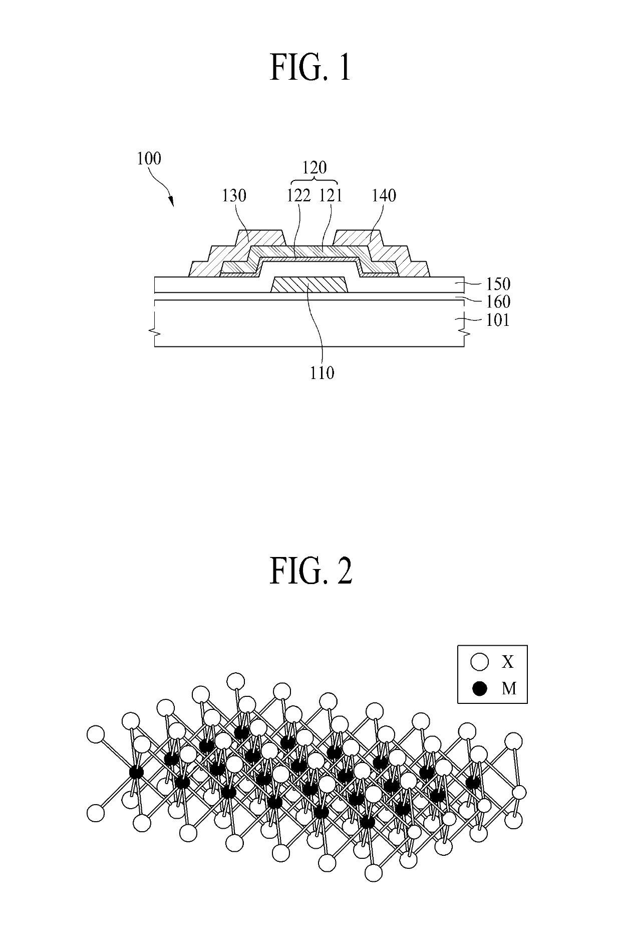
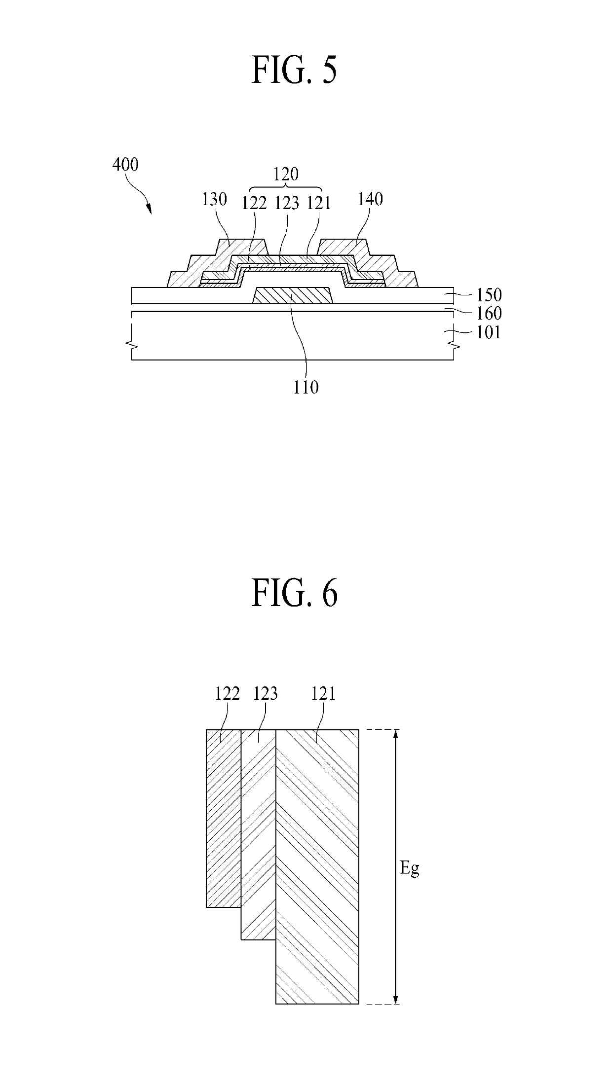
[0161]A gate electrode 110 composed of an alloy of Mo and Ti and having a thickness of 100 nm was formed on a substrate 101 made of glass, a gate insulation film 150 made of a silicon oxide was formed on the gate electrode 110, and a semiconductor layer 120 was formed on the gate insulation film 150. Specifically, a second layer 122, which is a two-dimensional semiconductor layer composed of molybdenum ditelluride (MoTe2) and having a dual-layer structure, was formed on the gate electrode 110, a third layer 123, which is a two-dimensional semiconductor layer composed of molybdenum disulfide (MoS2) and having a single-layer structure, was formed on the second layer 122, and a first layer 121, which is an oxide semiconductor layer including indium (In), gallium (Ga), and zinc (Zn) in a ratio of 1:1.5:1 and having a thickness of 30 nm, was formed on the third layer 123, whereby the semiconductor layer 120 was formed. Subsequently, a source electrode 130 having a thickness of 100 nm and...
PUM
| Property | Measurement | Unit |
|---|---|---|
| energy band gap | aaaaa | aaaaa |
| energy band gap | aaaaa | aaaaa |
| thickness | aaaaa | aaaaa |
Abstract
Description
Claims
Application Information