Chip on glass type liquid crystal display device and method for fabricating the same

a liquid crystal display device and glass-type technology, applied in semiconductor devices, instruments, sold ingredients supply devices, etc., can solve the problems of less deformation and inability to accurately drive the liquid crystal display device, and achieve the effect of increasing the contact surface area and preventing non-conta

Active Publication Date: 2005-11-03
LG DISPLAY CO LTD
View PDF9 Cites 19 Cited by
  • Summary
  • Abstract
  • Description
  • Claims
  • Application Information

AI Technical Summary

Benefits of technology

[0032] In one aspect, the drive ICs and the FPC film are packaged on the substrate at the same time in the display device. Since the surface of the pad electrode where the FPC film is attached is embossed, it is possible to prevent non-contact that is caused by the step non-uniformity between the pad electrodes.

Problems solved by technology

Consequently, the driving of the liquid crystal display device is not achieved correctly.
These problems occur more often under a high-temperature high-humidity environment because the adhesive state of the ACF 84 is more degraded in that condition.

Method used


Image

  • Chip on glass type liquid crystal display device and method for fabricating the same
  • Chip on glass type liquid crystal display device and method for fabricating the same
  • Chip on glass type liquid crystal display device and method for fabricating the same

Examples


Embodiment Construction

[0045] Reference will now be made in detail to the preferred embodiments of the present invention, examples of which are illustrated in the accompanying drawings. Wherever possible, the same reference numbers will be used throughout the drawings to refer to the same or like parts.

[0046]FIG. 3 is a plan view of a liquid crystal display device according to a first embodiment of the present invention; FIG. 4 is a sectional view taken along line II-II′ of FIG. 3; FIGS. 5A and 5B are sectional views illustrating a process of attaching an FPC film according to the present invention; and FIG. 7 is a plan view of a liquid crystal display device according to a second embodiment of the present invention.

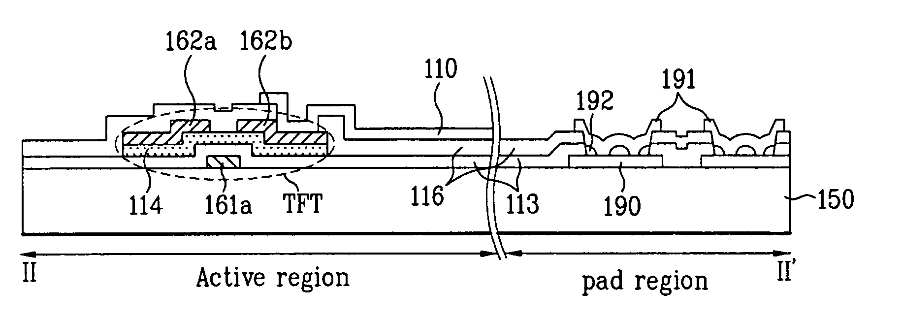
[0047] Referring to FIGS. 3 and 4, a TFT array substrate 150 where TFTs are formed is divided into an active region 152 and a pad region 154.

[0048] In the active region 152, gate lines 161 are formed to transfer a scanning signal. Also, data lines 162 are vertically intersected with the gat...


PUM

PropertyMeasurementUnit
transparentaaaaaaaaaa
transparent conductiveaaaaaaaaaa
insulatingaaaaaaaaaa

Abstract

A chip on glass type liquid crystal display device and a method for fabricating the same are provided in which a surface of a pad electrode for attaching a flexible printed circuit film is embossed to increase an adhesive force between a pad electrode and a flexible printed circuit film, thereby ensuring contact between the pad electrode and the flexible printed circuit film. Unit pixels in an active region contain thin film transistors formed at intersections of gate lines and data lines. A pad electrode is formed in an inactive region. An embossing pattern is formed on the pad electrode. An adhesive is provided on the pad electrode including the embossing pattern and an external drive circuit part is connected to the pad electrode by the adhesive.

Description

[0001] This application claims the benefit of the Korean Application No. P2004-29430 filed on Apr. 28, 2004, which is hereby incorporated by reference. FIELD OF THE INVENTION [0002] The present invention relates to a liquid crystal display device, and more particularly, to a chip on glass type liquid crystal display device and a method for fabricating the same, in which adhesive force between a pad electrode of a substrate and a flexible printed circuit film is enhanced. DISCUSSION OF THE RELATED ART [0003] A liquid crystal display device has large contrast ratio and low power consumption such that it is adapted to represent a gray scale and display a moving picture. For these reasons, the liquid crystal display device is widely used as a flat display device. [0004] The liquid crystal display device includes a color filter substrate having a color filter layer for color representation, a thin film transistor (TFT) array substrate facing the color filter substrate, a liquid crystal l...

Claims


Application Information

Patent Timeline
Patent Type & Authority Applications(United States)
IPC IPC(8): G02F1/1345G02F1/13G02F1/136G02F1/1362H01L27/12
CPCG02F1/13452H01L27/12G02F1/13458B28C7/003B28C7/06B65G47/61
Inventor JUNG, TAE WOO
Owner LG DISPLAY CO LTD
Why Eureka
Try Eureka