

Complementary metal oxide semiconductor image sensor and method for fabricating the same
a metal oxide semiconductor and image sensor technology, applied in the direction of discharge tube/lamp details, instruments, discharge control devices, etc., can solve the problems of limited full factor, deterioration of cmos image sensor characteristics, and restrictions on effective avoidance of cross talk, so as to effectively minimize cross talk and effectively minimize the effect of cross talk
- Summary
- Abstract
- Description
- Claims
- Application Information
AI Technical Summary
Benefits of technology
Problems solved by technology
Method used
Image

Examples
Embodiment Construction
[0024] Reference will now be made in detail to exemplary embodiments of the invention, examples of which are illustrated in the accompanying drawings. Wherever possible, the same reference numbers will be used throughout the drawings to refer to the same or like parts.
[0025] An embodiment of the present invention will now be described in detail with reference to the accompanying drawings.
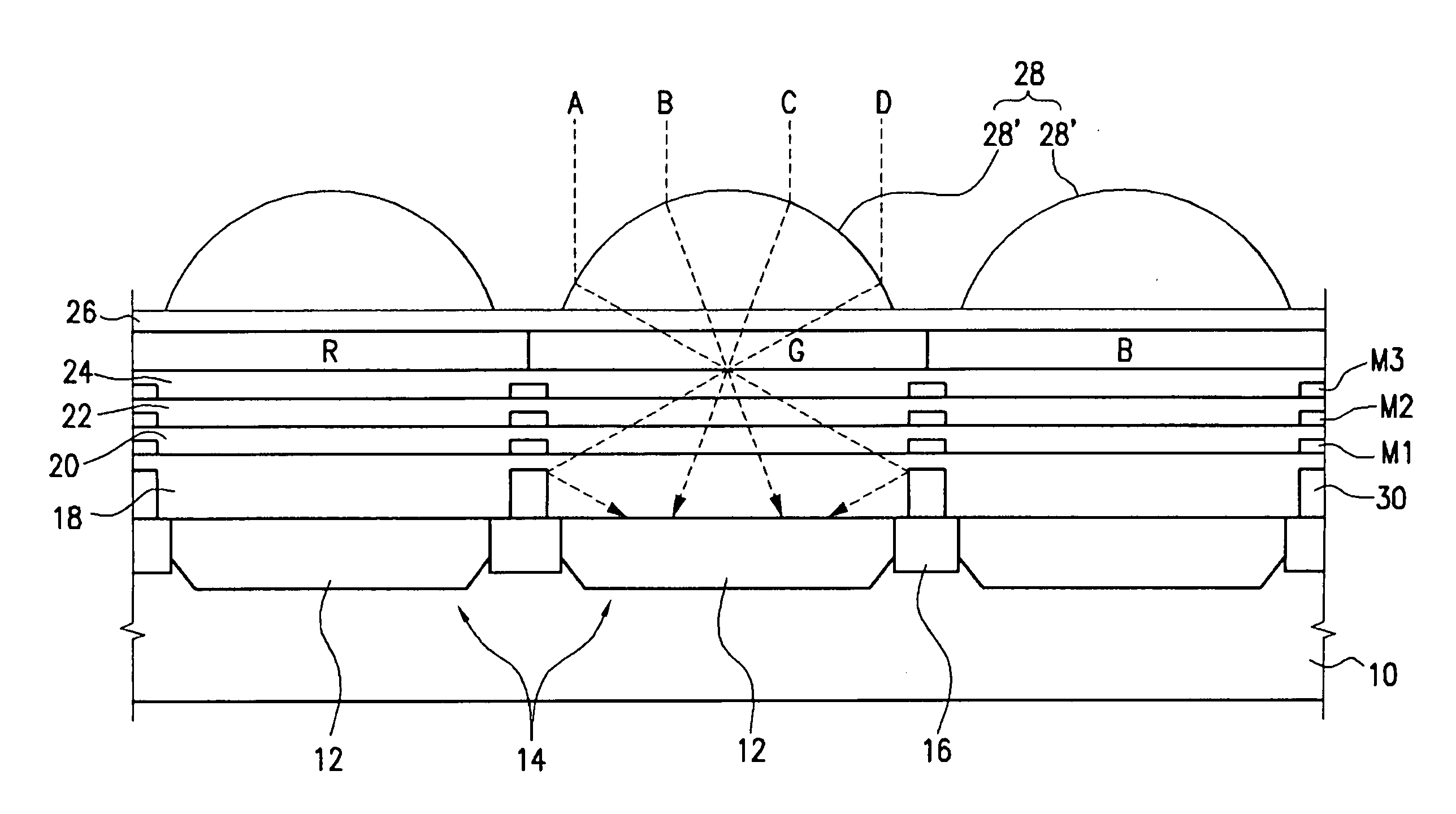
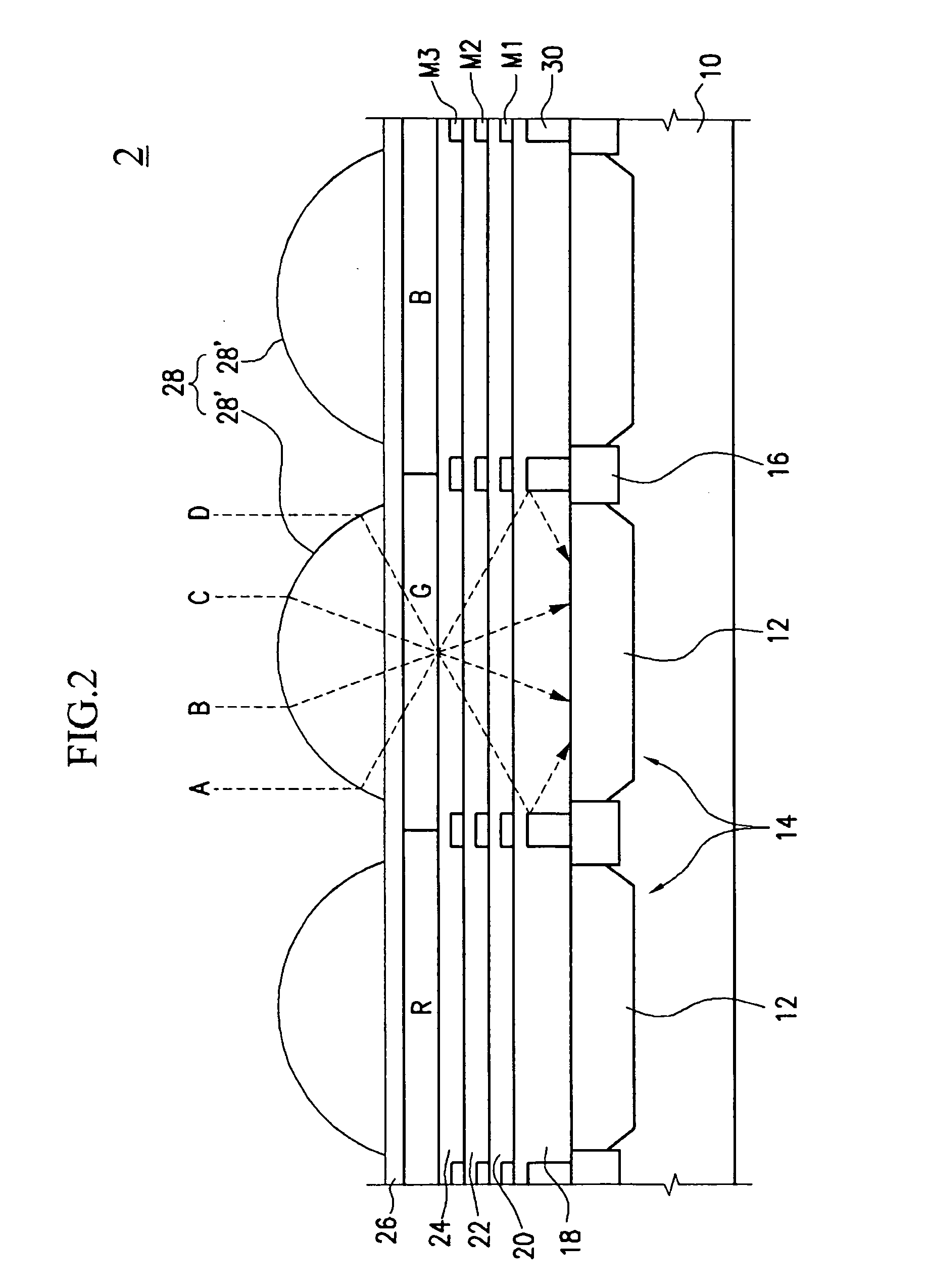
[0026]FIG. 2 is a schematic sectional view illustrating a CMOS image sensor 2 consistent with an embodiment of the present invention.
[0027] Referring to FIG. 2, CMOS image sensor 2 includes a semiconductor substrate 10 on which CMOS devices 14 are formed. CMOS devices 14 include photocharge generating portions 12 for receiving light externally and for generating and accumulating charges. In one aspect, photocharge generating portions 12 comprise photodiodes each formed as an impurity junction layer, with one photodiode provided per pixel.
[0028] In addition, CMOS devices 14 are formed in a plural...
PUM
 Abstract
Description
Claims
Application Information