Ultra-thin die and method of fabricating same

a technology of ultra-thin dies and dies, applied in the field of ultra-thin dies, can solve the problems of only being able to accommodate die thinning only so much, and the likelihood of further damage to the di

Active Publication Date: 2006-01-05
TAIWAN SEMICON MFG CO LTD
View PDF26 Cites 48 Cited by
  • Summary
  • Abstract
  • Description
  • Claims
  • Application Information

AI Technical Summary

Problems solved by technology

However, grinding alone can accommodate die thinning only so much before the mechanical forces involved chip or break semiconductor wafers.
During the separate process of singulating the die, there is a likelihood of causing further damage to the die, especially when they are in a thinned state.

Method used


Image

  • Ultra-thin die and method of fabricating same
  • Ultra-thin die and method of fabricating same
  • Ultra-thin die and method of fabricating same

Examples


Embodiment Construction

)

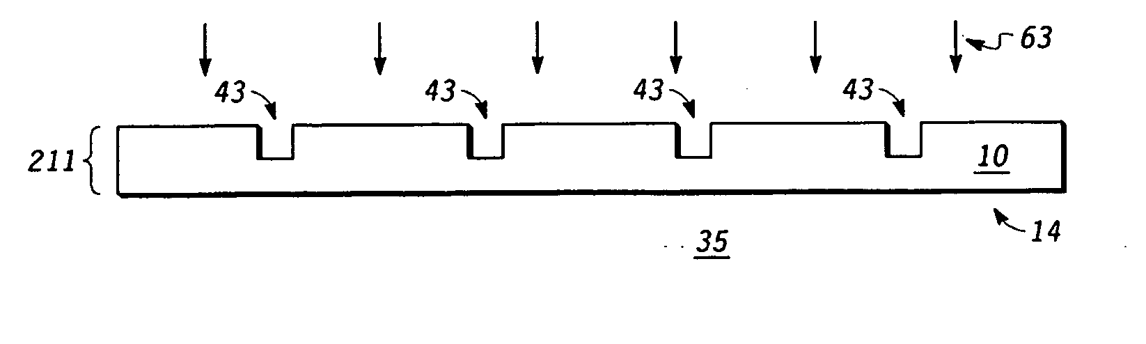
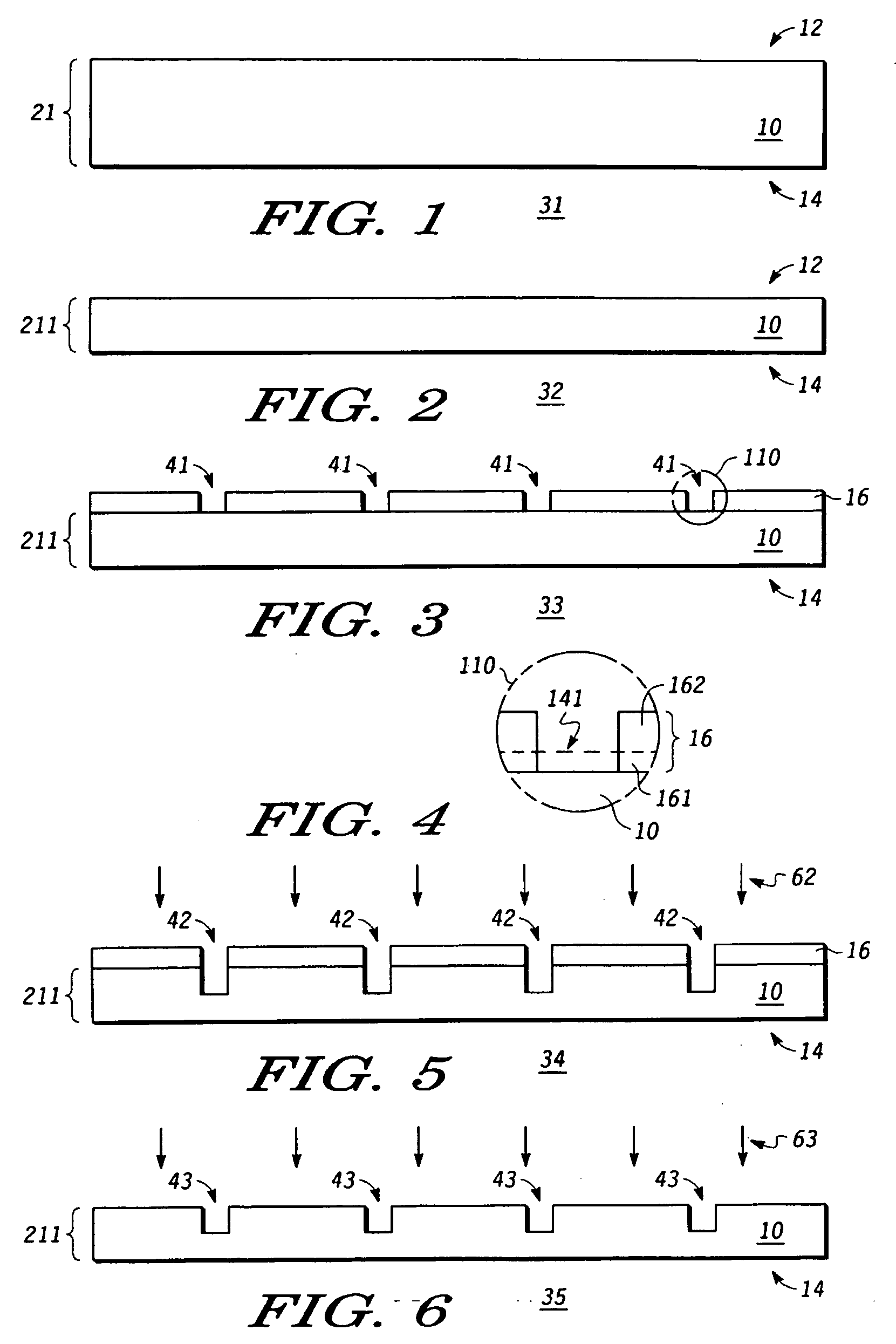
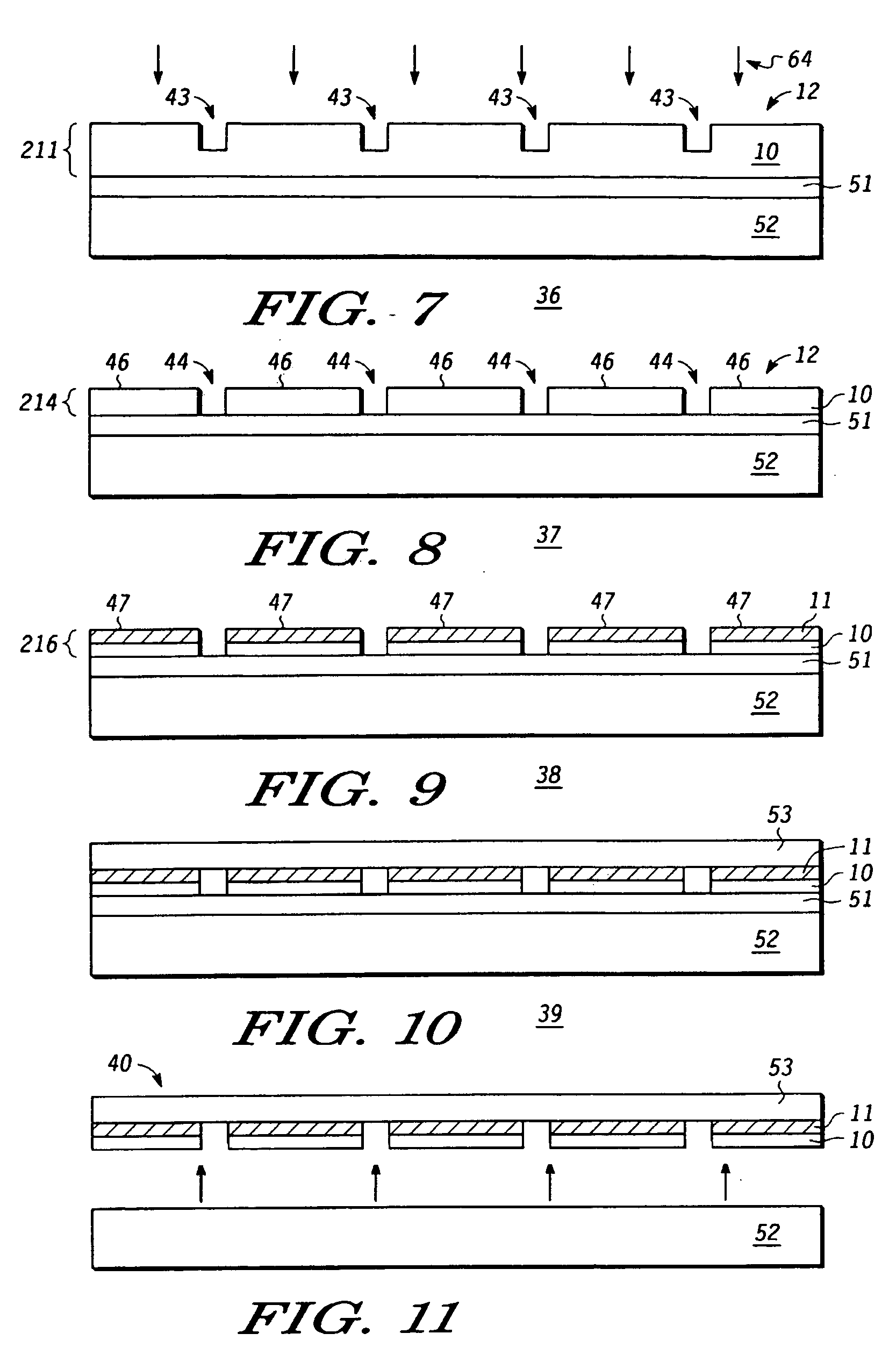
[0009] In accordance with a specific embodiment of the present disclosure, a method of processing a semiconductor substrate is disclosed whereby the substrate is both thinned and diced (singulated) during a common process. In one embodiment, a mask layer, such as a photoresist or other patternable organic layer having open trench regions, is formed on the backside of the substrate using standard lithography coupled with backside alignment techniques. The trench regions are typically aligned to scribe grid regions defined on the frontside of the substrate. An anisotropic etch applied to the backside results in a pattern transfer of the trench regions onto the backside of the substrate. After the mask layer is removed, either by etch consumption or stripping, etch of the backside of the substrate is performed to thin the wafer evenly over the backside surface. The trench areas, which constitute the deepest portion of the backside are etched simultaneously and remain the deepest porti...


PUM


Abstract

In accordance with a specific embodiment, a method of processing a semiconductor substrate is disclosed whereby the substrate is thinned, and the dice formed on the substrate are singulated by a common process. Trench regions are formed on a backside of the substrate. An isotropic etch of the backside results in a thinning of the substrate while maintaining the depth of the trenches, thereby facilitating singulation of the die.

Description

BACKGROUND [0001] 1. Field of the Disclosure [0002] The present disclosure relates to semiconductor devices and more particularly to methods related to reducing the thickness of semiconductor devices. [0003] 2. Description of the Related Art [0004] Empirical studies and computer models have demonstrated that the performance of a semiconductor device can be improved by thinning the semiconductor die. The method used most commonly to thin the die is a back grinding procedure done prior to die sawing or singulation. However, grinding alone can accommodate die thinning only so much before the mechanical forces involved chip or break semiconductor wafers. In addition, subsequent to the back-grind process, the individual die formed on the wafer are singulated using a saw cutting or scribing technique. During the separate process of singulating the die, there is a likelihood of causing further damage to the die, especially when they are in a thinned state. Therefore, a method of overcoming...

Claims


Application Information

Patent Timeline
Patent Type & Authority Applications(United States)
IPC IPC(8): H01L21/301H01L21/46
CPCH01L21/3065Y10S438/977H01L21/78
Inventor MANCINI, DAVID P.CHUNG, YOUNG SIRDAUKSHER, WILLIAM J.WESTON, DONALD F.YOUNG, STEVEN R.BAIRD, ROBERT W.
Owner TAIWAN SEMICON MFG CO LTD
Why Eureka
Try Eureka