

Ultra-fast nucleic acid sequencing device and a method for making and using the same
a nucleic acid and ultra-fast technology, applied in semiconductor/solid-state device testing/measurement, instruments, material electrochemical variables, etc., can solve the problems of limiting analysis of strands to a length of 500 bases, unable to perform rapid length determination, and inability to accurately and effectively identify individual bases of dna or rna
- Summary
- Abstract
- Description
- Claims
- Application Information
AI Technical Summary
Benefits of technology
Problems solved by technology
Method used
Image

Examples
Embodiment Construction
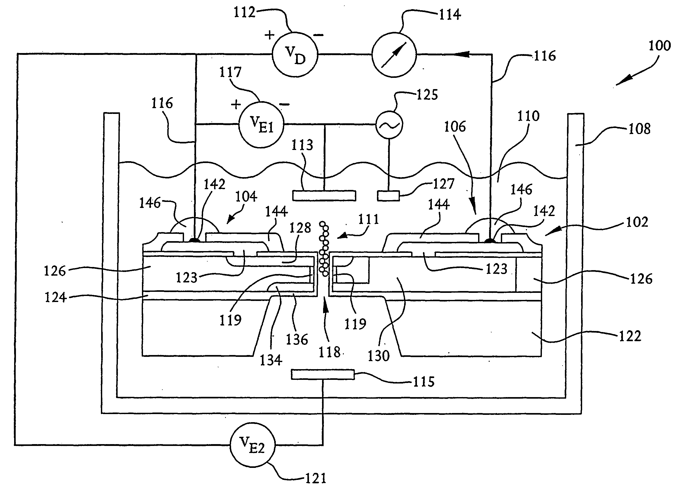
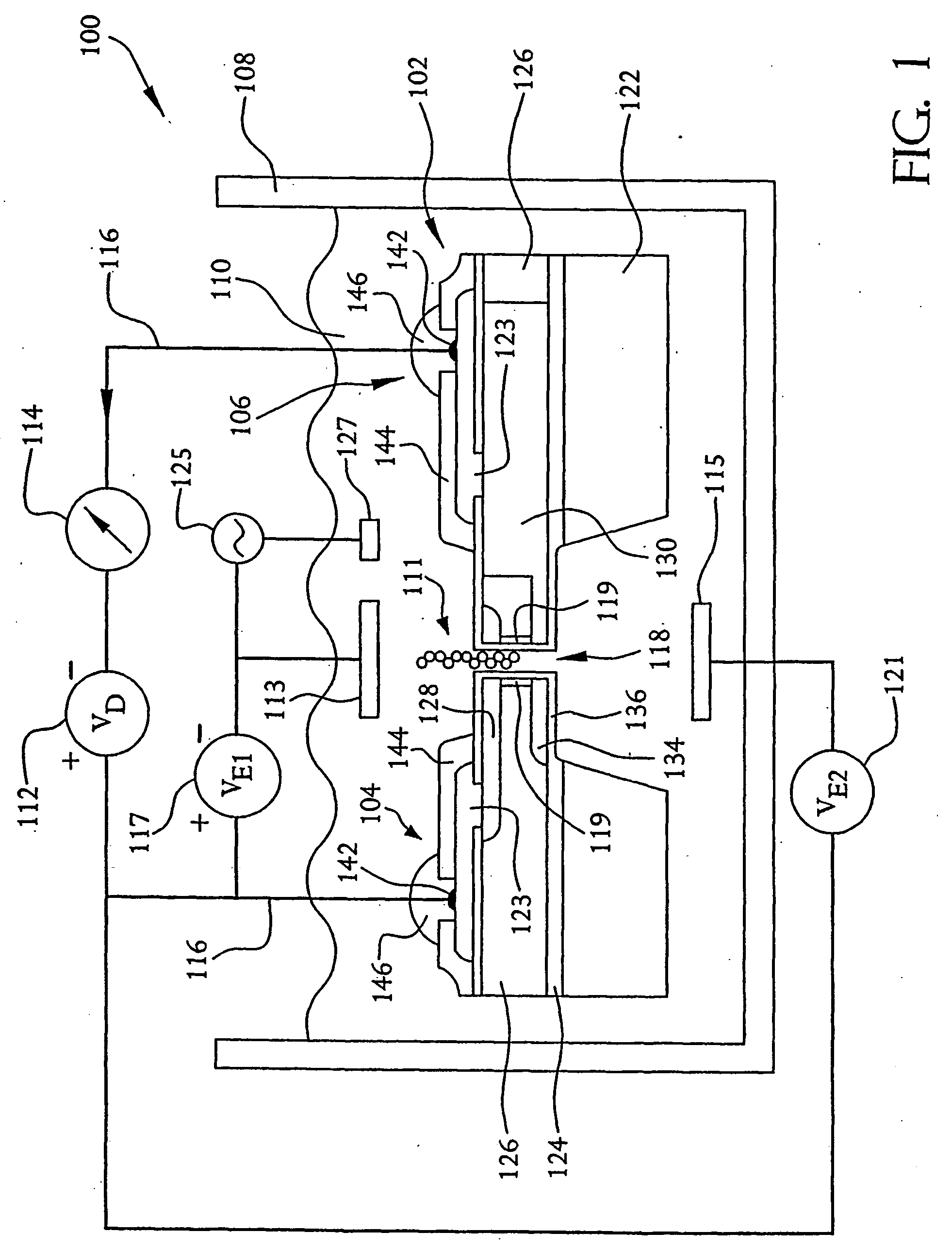
[0050]FIGS. 1 and 2 illustrate a system 100 for detecting the presence of a polymer, such as DNA or RNA, a protein or carbohydrate, or a long chain polymer such as petroleum, and, more preferably, for identifying the individual mers of the polymer or long chain polymer, as well as the length of the polymer or long chain polymer. The system 100 is preferably adaptable for performing sequencing of nucleic acids, such as DNA or RNA sequencing, according to an embodiment of the present invention. Accordingly, for purposes of this description, the system 100 will be discussed in relation to nucleic acid sequencing.
[0051] The system 100 includes a nucleic acid sequencing device 102 which, as described in more detail below, is a semiconductor device. Specifically, the nucleic acid sequencing device 102 resembles a field-effect transistor, such as a MOSFET, in that it includes two doped regions, a drain region 104 and a source region 106. However, unlike a MOSFET, the nucleic acid sequenci...
PUM
| Property | Measurement | Unit |
|---|---|---|
| voltage potential | aaaaa | aaaaa |
| frequency | aaaaa | aaaaa |
| diameter | aaaaa | aaaaa |
Abstract
Description
Claims
Application Information