Relaxation oscillator based keypad decoder
a relaxation oscillator and keypad technology, applied in the direction of coding, instruments, pulse techniques, etc., can solve the problem of not being able to attach each button to a digital input, and achieve the effect of a simple digital keypad processor
- Summary
- Abstract
- Description
- Claims
- Application Information
AI Technical Summary
Benefits of technology
Problems solved by technology
Method used
Image
Examples
first embodiment
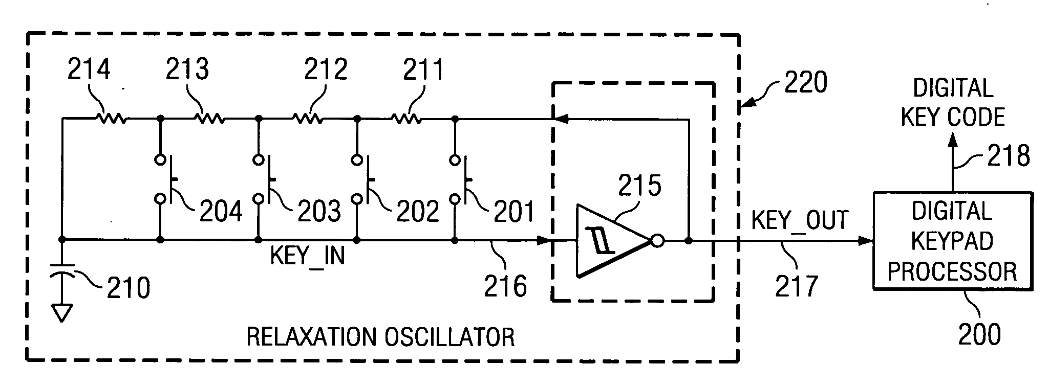
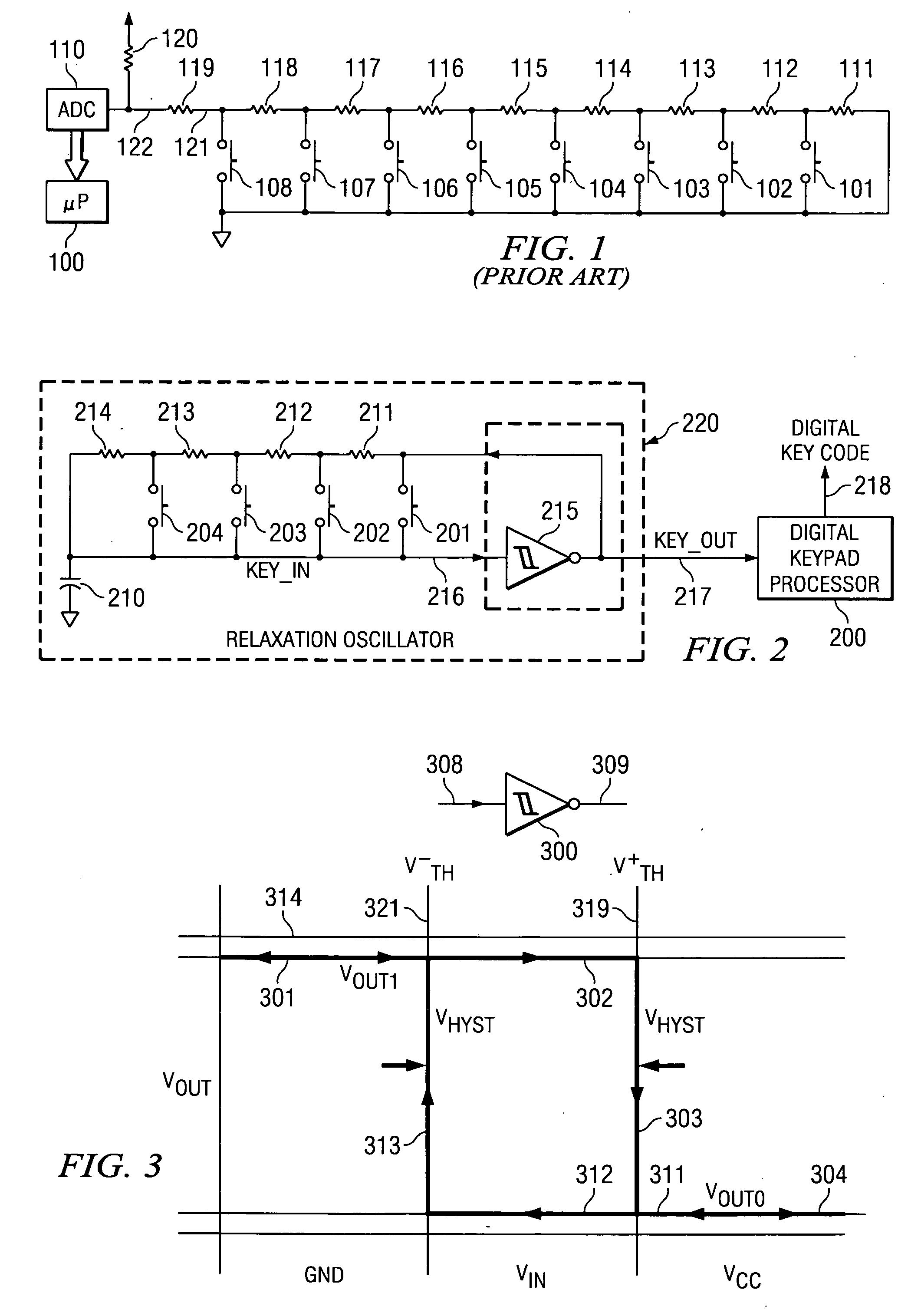
[0019]FIG. 2 illustrates the keypad decoder of this invention including relaxation oscillator 220 and digital keypad processor 200. Relaxation oscillator 220 converts pushbutton inputs into a square wave output whose frequency varies depending on the button or buttons pressed. Digital keypad processor 200 measures and records the period of the relaxation oscillator waveform and send the measured period output to a host processor as digital key code 218. This measured period output is mapped by software into a respective key-code.
Relaxation Oscillator
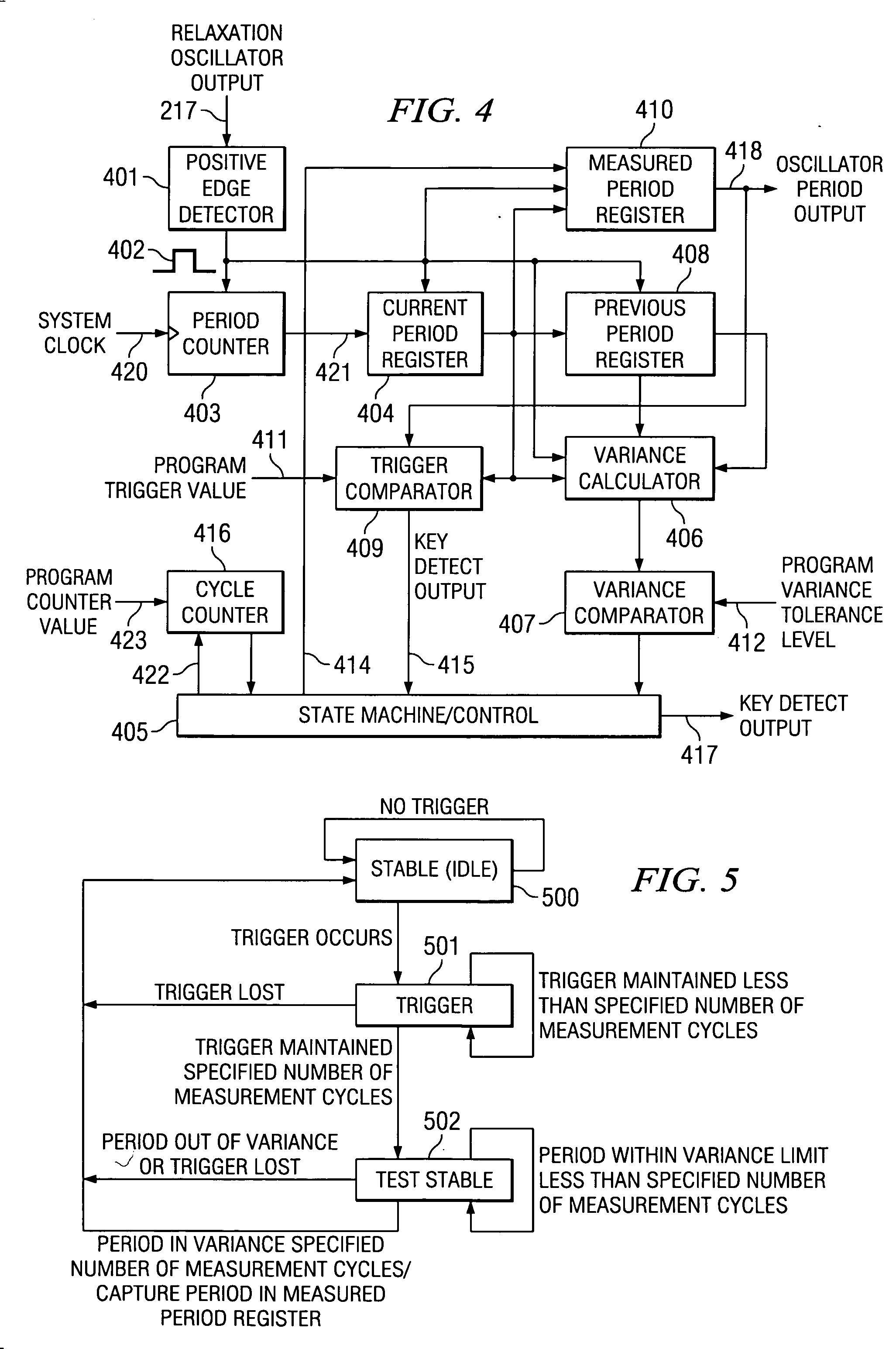
[0020] Relaxation oscillator 220 generates a square wave variable frequency waveform. CMOS inverter circuit 215, the active element of relaxation oscillator 220, has a double-valued input threshold voltage that is dependent upon the direction of input voltage variations. The resulting transfer characteristic is commonly referred to as one having hysteresis. FIG. 2 illustrates a first embodiment of a plurality of possible relaxation osci...
third embodiment
[0051]FIG. 7 illustrates the invention. The pushbuttons are organized into two banks of five pushbuttons. The relaxation oscillator of FIG. 7 also includes capacitor 710 and hysteresis inverter 700. All single key-presses can be detected as well as any input combination where one pushbutton from bank A including pushbuttons 721, 722, 723, 724 and 725 and another from bank B including pushbuttons 741, 742, 743, 744 and 745 is depressed. The resistors of bank A all have the value R. The resistors of bank B all have the value 6R, which is the sum of all resistors of bank A. Note that equal number of pushbuttons in bank A and bank B is not required. FIG. 7 merely illustrates an example where there are five pushbuttons in bank A and 5 pushbuttons in bank B. Table 2 summarizes the relationship between the pushbutton input and the resulting period for the circuit of FIG. 7.
TABLE 2CombinationsS1S2S3S4S5OpenS6 1T 2T 3T 4T 5T 6TS7 7T 8T 9T10T11T12TS813T14T15T16T17T18TS919T20T21T22T23T24T S102...
PUM
 Abstract
Description
Claims
Application Information


