

Liquid crystal display panel and fabricating method thereof
- Summary
- Abstract
- Description
- Claims
- Application Information
AI Technical Summary
Benefits of technology
Problems solved by technology
Method used
Image

Examples
first embodiment
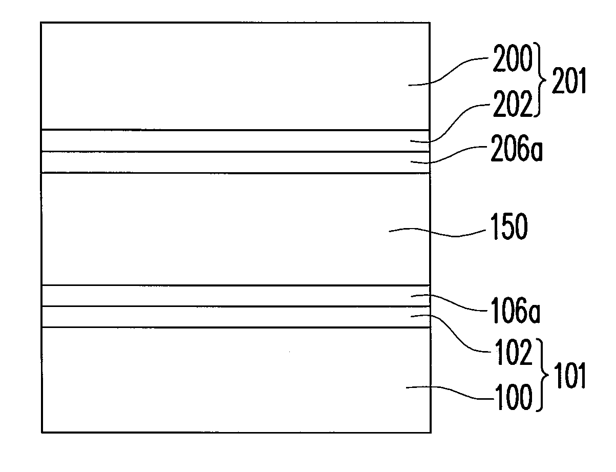
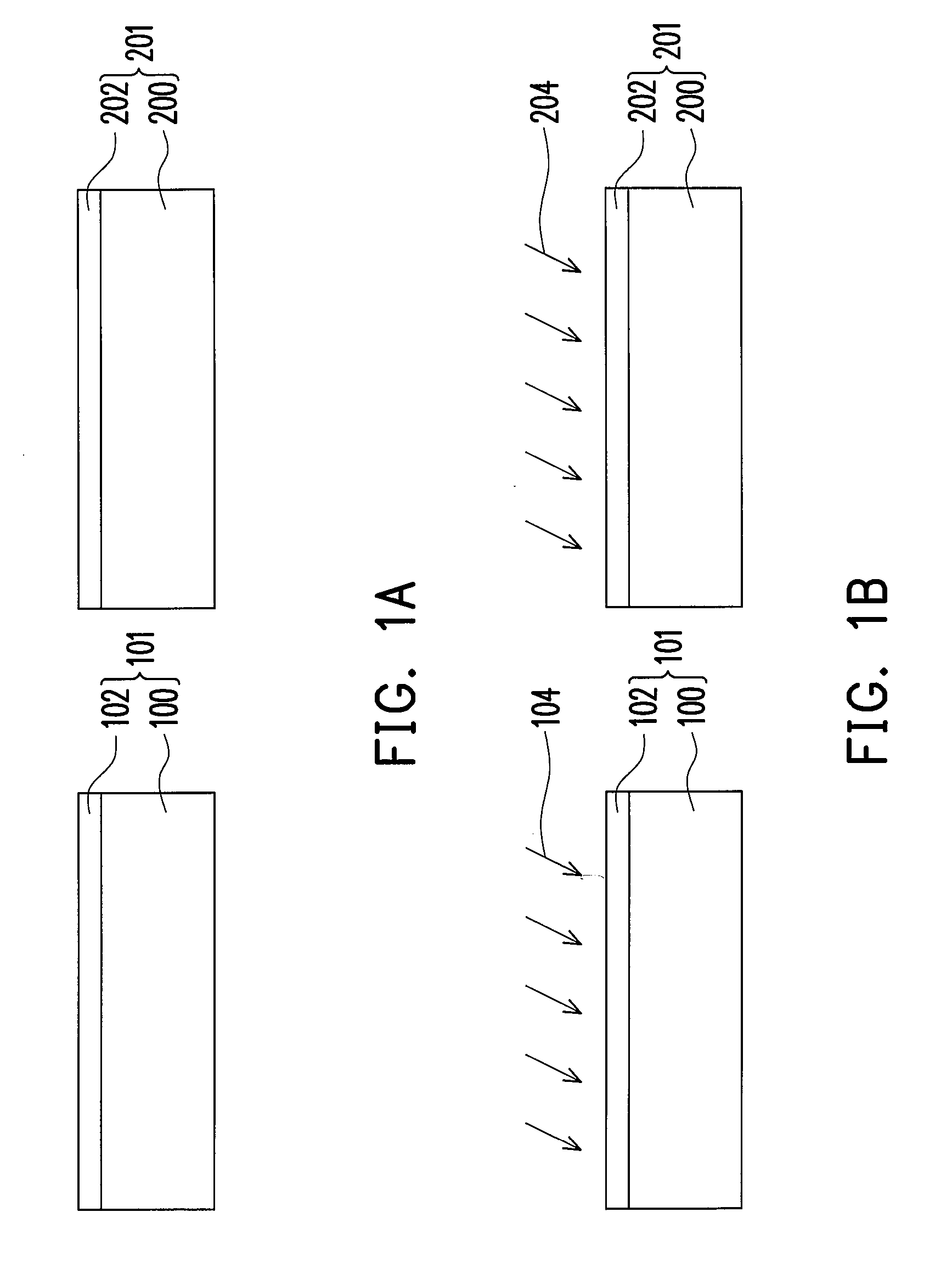
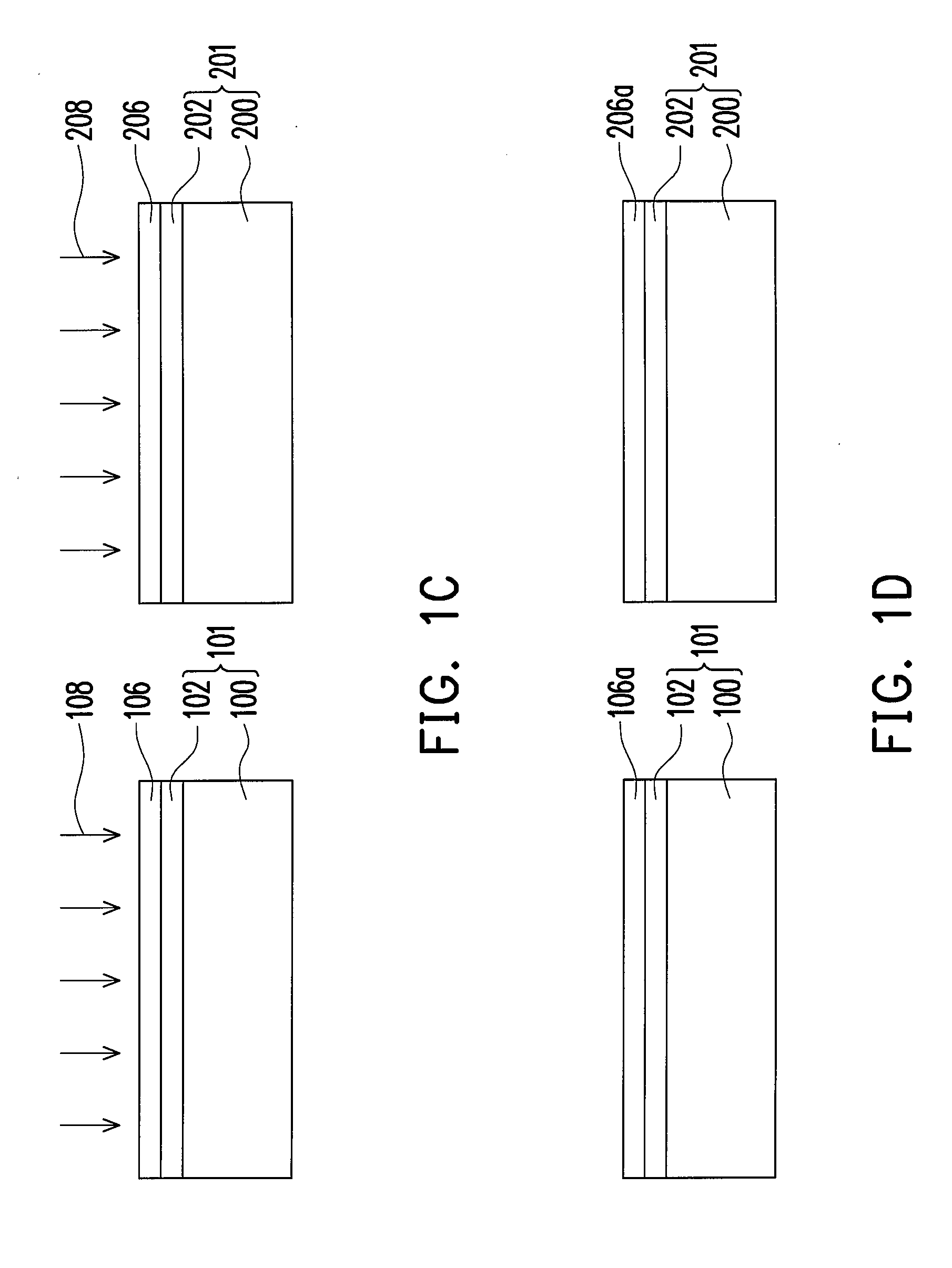
[0019]FIGS. 1A˜1E are cross-sectional views illustrating the fabricating flow of a liquid crystal display (LCD) panel according to the first embodiment of the present invention. Referring to FIG. 1A, the first substrate 101 is composed of the substrate 100 and a film layer 102 formed on the substrate 100, and the second substrate 201 is composed of the substrate 200 and a film layer 202 formed on the substrate 200. The substrates 100 and 200 may be glass substrates, silicon substrates, flexible plastic substrates, or any existing substrate which can be used for fabricating display panel. If the display panel in the present invention is a passive matrix display panel, then film layer 102 and film layer 202 may be respectively an electrode layer. If the display panel in the present invention is an active matrix display panel, then film layer 102 may be an active matrix device layer, and film layer 202 may be a common electrode layer. The material of the electrode layer may be organic ...
second embodiment
[0028]FIGS. 2A-2E are cross-sectional views illustrating the fabricating flow of a LCD panel according to the second embodiment of the present invention. Referring to FIG. 2A, a first substrate 101 and a second substrate 201 are provided first. The composition and material of the first substrate 101 and the second substrate 201 are as those described in the first embodiment, therefore will not be described herein. Next, a first alignment material layer 120 and a second alignment material layer 220 are respectively formed on the surfaces of the first substrate 101 and the second substrate 201. The first and the second alignment material layers 120 and 220 may be an organic alignment material or an inorganic alignment material. In an embodiment, the organic alignment material includes poly vinyl alcohol, polyimide, polyamic acid, azo-benzene, poly vinyl cinnamate, compound containing coumarin group, compound containing chalcone group, or other existing organic alignment material. In a...
PUM
| Property | Measurement | Unit |
|---|---|---|
| Electrical conductor | aaaaa | aaaaa |
Abstract
Description
Claims
Application Information