

Power MISFET, semiconductor device and DC/DC converter
a technology of power misfet and semiconductor device, which is applied in the direction of electric variable regulation, process and machine control, instruments, etc., can solve the problems of self-turning, reduction of resistance (ron) required to the power misfet, and loss of conductan
- Summary
- Abstract
- Description
- Claims
- Application Information
AI Technical Summary
Benefits of technology
Problems solved by technology
Method used
Image

Examples
first embodiment
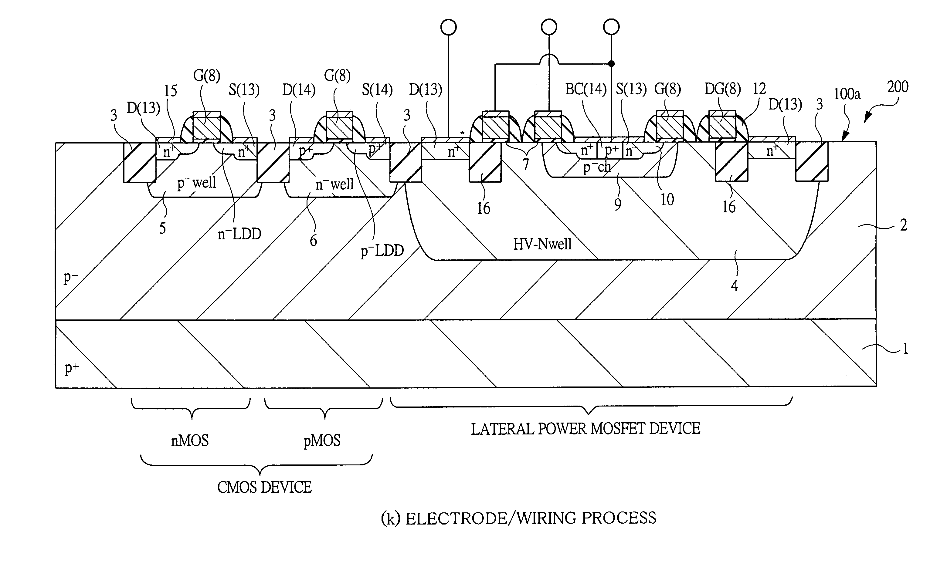
[0056]In a first embodiment, as an example of a power MISFET, a lateral power MOSFET in which a source region, a channel region, a drift region and a drain region are arranged in sequence along one main surface of a semiconductor substrate, will be described as an instance.
[0057]FIG. 1 is a perspective view showing a cross sectional structure of main parts of an n-type lateral power MOSFET according to the first embodiment.
[0058]In FIG. 1, the lateral power MOSFET 100 comprises a p+ substrate 1 of p-type (first conducting type) and a first impurity concentration. Further, on the p+ substrate 1, a p− epitaxial layer 2 of the first conducting type and a second impurity concentration lower than the first impurity concentration is arranged. In other words, the lateral power MOSFET 100 has a semiconductor substrate formed of the p+ substrate 1 and the p− epitaxial layer 2.
[0059]Further, on the p− epitaxial layer 2, an Nwell (hereinafter, referred to as “well”) layer 4 of n-type (second c...
second embodiment
[0116]FIG. 20 is a perspective view showing a structure of a lateral power MOSFET 300 according to a second embodiment of the present invention. A feature of the second embodiment is that the source layer S and the body contact layer BC are arranged alternately along a second direction intersecting with a first direction which is the arrangement direction of the source layer S, the gate electrode G and the drain layer D.
[0117]By arranging the source layer S and the body contact layer BC alternately along the second direction, it is possible to make the cell size further smaller than in the lateral power MOSFET 100 described in the first embodiment. Further, by making the cell size smaller, it is possible to reduce the ON resistance.
third embodiment
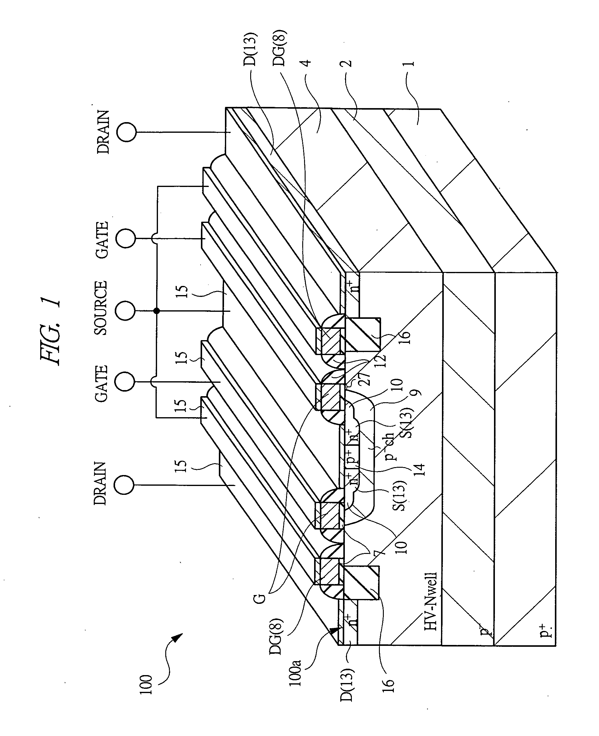
[0118]FIG. 21 is a cross-sectional view showing a structure of a lateral power MOSFET 400 according to a third embodiment of the present invention. A feature of the third embodiment is that the trench region 16 in a drift region of the lateral power MOSFET 400 is shallower than the STI region for device isolation (the first device isolation region and the second device isolation region) 3.
[0119]As shown in FIG. 21, the lateral power MOSFET 400 has a CMOS device structured by an nMOS device and a pMOS device, and a lateral power MOSFET device in a same chip. Between the lateral power MOSFET device and the CMOS device, the STI region 3 as a first device isolation region is formed. Further, between the nMOS device and the PMOS device structuring the CMOS device, the STI region 3 as a second device isolation region is formed.
[0120]Furthermore, the depth in a direction from the main surface 100a of the STI region 3 formed in the HV-Nwell layer 4 as the drift region of the lateral power M...
PUM
 Abstract
Description
Claims
Application Information