Light Emitting Element and Light Emitting Device

a technology of light emitting elements and light emitting devices, which is applied in the direction of discharge tubes/lamp details, luminescent screens, discharge tubes/lamp details, etc., can solve the problems of high voltage needed to apply current, high voltage for obtaining luminance (that is, driving voltage), and difficult to flow current, etc., to achieve easy prevention of short circuit and reduce driving voltage

Inactive Publication Date: 2008-10-16
SEMICON ENERGY LAB CO LTD
View PDF3 Cites 15 Cited by
  • Summary
  • Abstract
  • Description
  • Claims
  • Application Information

AI Technical Summary

Benefits of technology

[0032]The practice of the present invention makes it possible to provide a light-emitting element that uses a material in which an organic compound and has a novel structure different from conventional structures, a light-emitting element that uses a material in which an organic compound and decreases in driving voltage, and a light-emitting element that uses a material in which an organic compound and easily prevents short circuit.

Problems solved by technology

Therefore, the light-emitting elements have a problem that current is hard to flow (that is, the voltage needed to apply a current gets higher) as compared with conventional organic EL elements.
In these light-emitting elements, since the luminance gets higher in proportion to an applied current density, the fact that current is hard to flow namely leads to a problem that the voltage for obtaining a luminance (that is, driving voltage) also gets higher.
Accordingly, when the organic compound is simply dispersed in the metal oxide, increase in driving voltage and increase in power consumption with the increase in driving voltage are caused even supposing that durability and heat resistance can be obtained.
Namely, in the conventional structure, it is difficult for practical purposes to make the film thickness thicker.

Method used


Image

  • Light Emitting Element and Light Emitting Device
  • Light Emitting Element and Light Emitting Device
  • Light Emitting Element and Light Emitting Device

Examples


embodiment mode 1

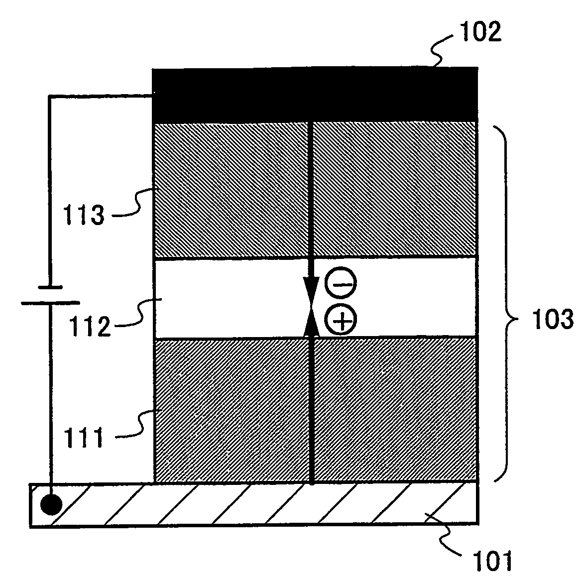
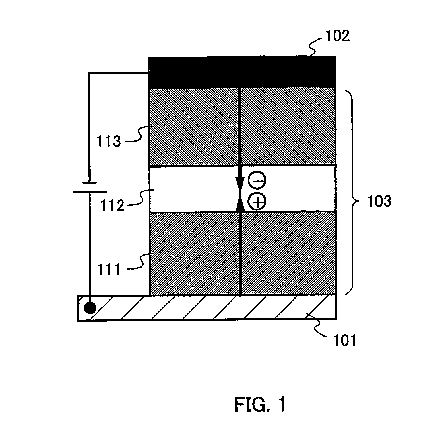
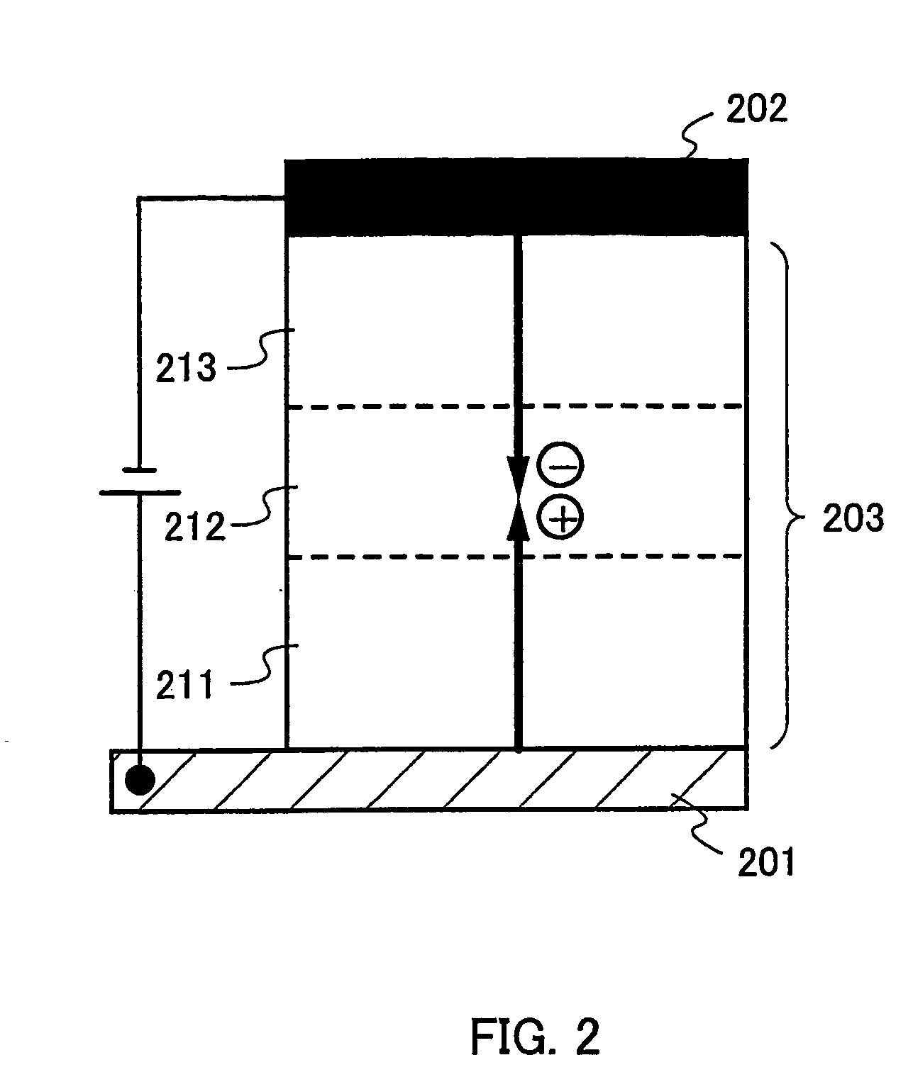
[0048]FIG. 1 shows the structure of a light-emitting element according to the present invention, where a composite layer 103 in which an organic compound and an inorganic compound are mixed is sandwiched between a first electrode 101 and a second electrode 102. The structure of the composite layer 103 is completely different from the structure of a composite layer 203 of a conventional light-emitting element (FIG. 2). The composite layer 103 has, as shown in the figure, a first layer 111, and a second layer 112, and a third layer 113, and in particular, the first layer 111 and the third layer 113 have significant features.

[0049]First, the first layer 111 is a layer that takes on the function of transporting holes to the second layer 112, and includes at least a first organic compound and a first inorganic compound that exhibits an electron accepting property to the first organic compound (serves as an electron acceptor). What is important is that the first inorganic compound is not ...

embodiment mode 2

[0072]In Embodiment Mode 2, an embodiment of a CEL element according to the present invention, which is different from Embodiment Mode 1, will be described. FIG. 5 shows the structure of the element. It is to be noted that the reference numerals in FIG. 1 are cited in FIG. 5.

[0073]FIG. 5 shows a light-emitting element sandwiching a composite layer 103 in which an organic compound and an inorganic compound are mixed between a first electrode 101 and a second electrode 102. As shown in the figure, the composite layer 103 includes a first layer 111, a second layer 112, a third layer 113, and a fourth layer 114.

[0074]Since the same structures as the respective layers in Embodiment Mode 1 (that is, FIG. 1) can be applied to the first electrode 101, the second electrode 102, the first layer 111, the second layer 112, and the third layer 113, explanations thereof are omitted. The thing that is different from Embodiment Mode 1 is that the fourth layer 114 is provided between the third layer...

embodiment mode 3

[0083]In the present embodiment mode, a light-emitting device that has a CEL element according to the present invention in a pixel portion will be described with reference to FIG. 8-(1) and 8-(2). FIG. 8-(1) is a top view showing the light-emitting device and FIG. 8-(2) is a cross-sectional view taken along A-A′ in FIG. 8-(2). Reference numeral 801 indicated by a dotted line denotes a source-side driver circuit, reference numeral 802 denotes a pixel portion, and reference numeral 803 denotes a gate-side driver circuit. In addition, reference numerals 804 and 805 denote a sealing substrate and a sealing material, respectively. A region 806 surrounded by the sealing material 805 may be a space filled with an inert gas or may be filled with a solid such as a resin.

[0084]A connecting wiring 807 for transmitting signals to be input to the source-side driver circuit 801 and the gate side driver circuit 803 receives signals such as a video signal, a clock signal, a start signal, and a rese...


PUM

PropertyMeasurementUnit
thicknessaaaaaaaaaa
work functionaaaaaaaaaa

Abstract

The present invention provides a light-emitting element sandwiching a composite layer in which an organic compound and an inorganic compound are mixed between a first electrode and a second electrode, where the composite layer includes a first layer including a first organic compound and a first inorganic compound that exhibits an electron accepting property to the first organic compound (serves as an electron acceptor), a second layer including a second organic compound and a second inorganic compound, and a third layer including a third organic compound and a third inorganic compound that exhibits an electron donating property to the third organic compound (serves as an electron acceptor).

Description

TECHNICAL FIELD[0001]The present invention relates to a light-emitting element, and more particularly to a light-emitting element including a composite layer in which an organic compound and an inorganic compound are mixed, and in addition, relates to a light-emitting device including a light-emitting element.BACKGROUND ART[0002]Recently, a light-emitting element that provides a high luminance by applying a current to an organic compound, such as a light-emitting element using a luminescent organic compound (referred to as an organic light-emitting diode [OLED] or an organic EL element, and hereinafter referred to as an organic EL element), has been getting a lot of attention.[0003]In the fundamental structure of an organic EL element, a layer including a luminescent organic compound (light-emitting layer) is sandwiched between a pair of electrodes. By applying a voltage to this element, electrons and holes are transported respectively from the pair of electrode to the light-emittin...

Claims


Application Information

Patent Timeline
Patent Type & Authority Applications(United States)
IPC IPC(8): H01L51/50H05B33/14
CPCH01L51/0059H01L51/0081H01L51/5012H01L51/5048H10K85/631H10K85/324H10K50/14H10K50/11H05B33/20H10K10/82H10K2102/301
Inventor YAMAZAKI, SHUNPEIIKEDA, HISAOSEO, SATOSHIKUMAKI, DAISUKESAKATA, JUNICHIRO
Owner SEMICON ENERGY LAB CO LTD
Why Eureka
Try Eureka