

Microstructures, method for producing microstructures, and optical field amplifying device
a microstructure and optical field technology, applied in the direction of optical radiation measurement, spectral modifiers, particle separator tubes, etc., can solve the problems of difficult stably holding the photosystem complex, the absorption efficiency of incident light is extremely low, and the bond between the metal particles that constitute the photosystem complex and the base materials is weak, so as to facilitate visual representation, improve detection sensitivity, and increase the size of the protruding portion
- Summary
- Abstract
- Description
- Claims
- Application Information
AI Technical Summary
Benefits of technology
Problems solved by technology
Method used
Image

Examples
first embodiment
of the Microstructure
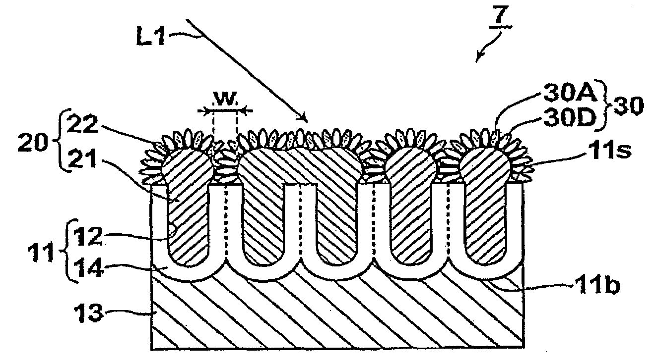
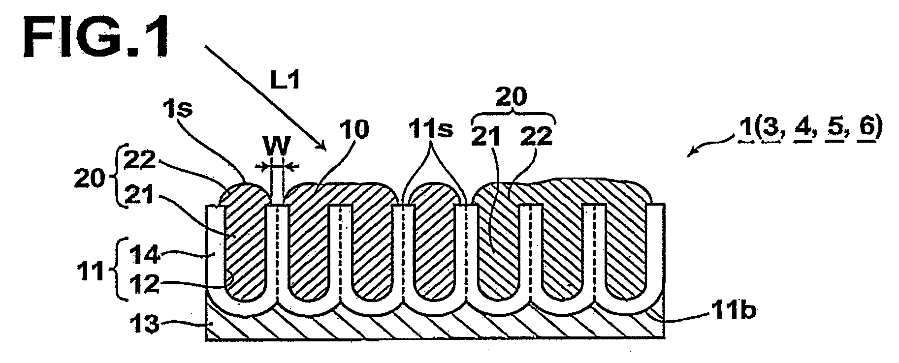
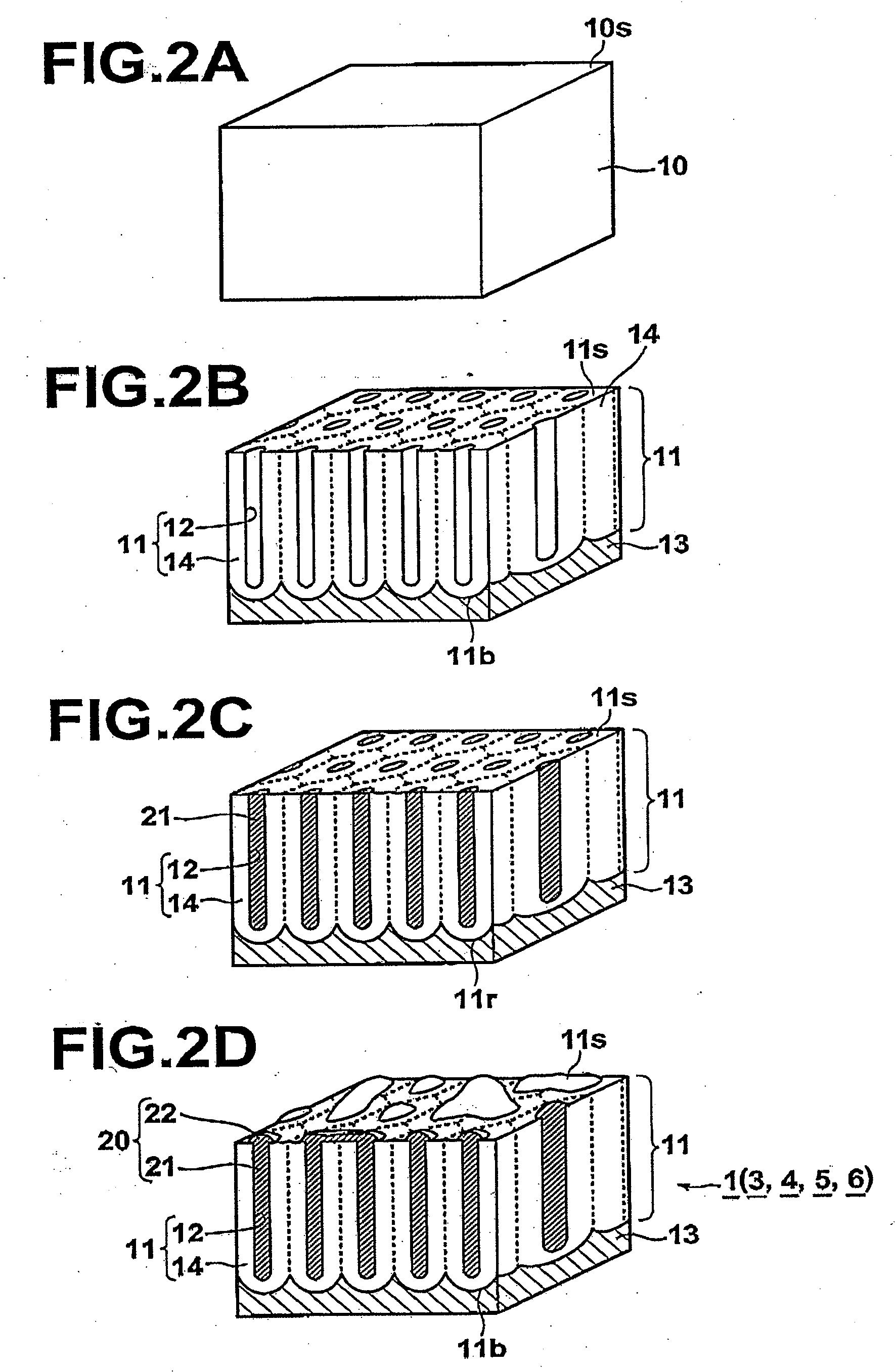
[0057]A microstructure 1 according to a first embodiment of the present invention will be described with reference to the drawings. FIG. 1 is a sectional view that illustrates the construction of the microstructure 1. FIG. 2 and FIG. 3 are diagrams that illustrate the manufacturing steps of the microstructure according to the first embodiment, wherein FIG. 2 shows perspective views of each step, and FIG. 3 shows sectional views of each step.
[0058]As illustrated in FIG. 1, the microstructure 1 is formed on a conductor 13, and is equipped with a dielectric base material 11 with a great number of regularly arranged fine holes 12, which are substantially the same shape in plan view, formed such that they are open at the surface 11s of the dielectric base material 11. A plurality of micro metal members 20, each of which have a filling portion 21 that fills one or more of the fine holes 12 and a protruding portion 22 that protrudes from the surface 11s of the base mat...
second embodiment
of the Microstructure
[0081]A microstructure 2 according to a second embodiment of the present invention will be described with reference to the drawings. FIG. 4 is a sectional view that illustrates the construction of the microstructure 2.
[0082]As illustrated in FIG. 4, the microstructure 2 is formed on a conductor 13, and is equipped with a dielectric base material 11 with a great number of regularly arranged fine holes 12, which are substantially the same shape in plan view, formed such that they are open at the surface 11s of the dielectric base material 11. A plurality of micro metal members 20, each of which have a filling portion 21 that fills one or more of the fine holes 12 and a protruding portion 22 that protrudes from the surface 11s of the base material 11 and is of a diameter, which is greater than the diameter of the filling portion, capable of inducing local plasmon, are fixed to the dielectric base material 11. In the second embodiment, the plurality of micro metal m...
example 1
[0108]The microstructure 1 of the first embodiment was produced by the following steps.
[0109]An aluminum plate (99.99% pure Al, at a thickness of 10 nm) was prepared as the metal material 10 to be anodized. The aluminum plate was used as an anode, and aluminum was used as a cathode, and anodization was performed under conditions that would result in a portion of the aluminum plate becoming an alumina layer 30. Thereby, the dielectric base material 11 and the conductor 13, which is a portion of the metal material 10 that was not anodized, were obtained. Anodization was performed according to the two step anodizing process disclosed in H. Masuda and M. Sato, “Fabrication of Gold Nanodot Array Using Anodic Porous Alumina as an Evaporation Mask”, J. J. Appl. Phys. Vol. 35, pp. L126-L129 (1996). The anodizing conditions were the same as those described in this document.
[0110]Next, the great number of fine holes 12 within the dielectric base material 11 were filled with Au by plating, usi...
PUM
| Property | Measurement | Unit |
|---|---|---|
| average distance | aaaaa | aaaaa |
| temperature | aaaaa | aaaaa |
| applied voltage | aaaaa | aaaaa |
Abstract
Description
Claims
Application Information