Wirelessly configurable memory device

a memory device and configurable technology, applied in the field of computing devices, can solve the problems of consuming a significant amount of power for transferring data via the traces and drivers, the basic architecture of random access memory is increasing in complexity, and the ability to reconfigure the architecture is reduced,

Inactive Publication Date: 2008-12-25
AVAGO TECH INT SALES PTE LTD
View PDF99 Cites 4 Cited by
  • Summary
  • Abstract
  • Description
  • Claims
  • Application Information

AI Technical Summary

Problems solved by technology

While a great many advances have been made in memory technology, once the architecture of a memory device is implemented on an IC, there is little ability to reconfigure the architecture.
In addition, as integrated circuit technology advances, the basic architecture of random access memory is increasing in complexity, capabilities, and size reduction.
As is known, the transferring of data via the traces and drivers consumes a significant amount of power, which produces heat, and consumes a relatively significant amount of die area.

Method used


Image

  • Wirelessly configurable memory device
  • Wirelessly configurable memory device
  • Wirelessly configurable memory device

Examples


Embodiment Construction

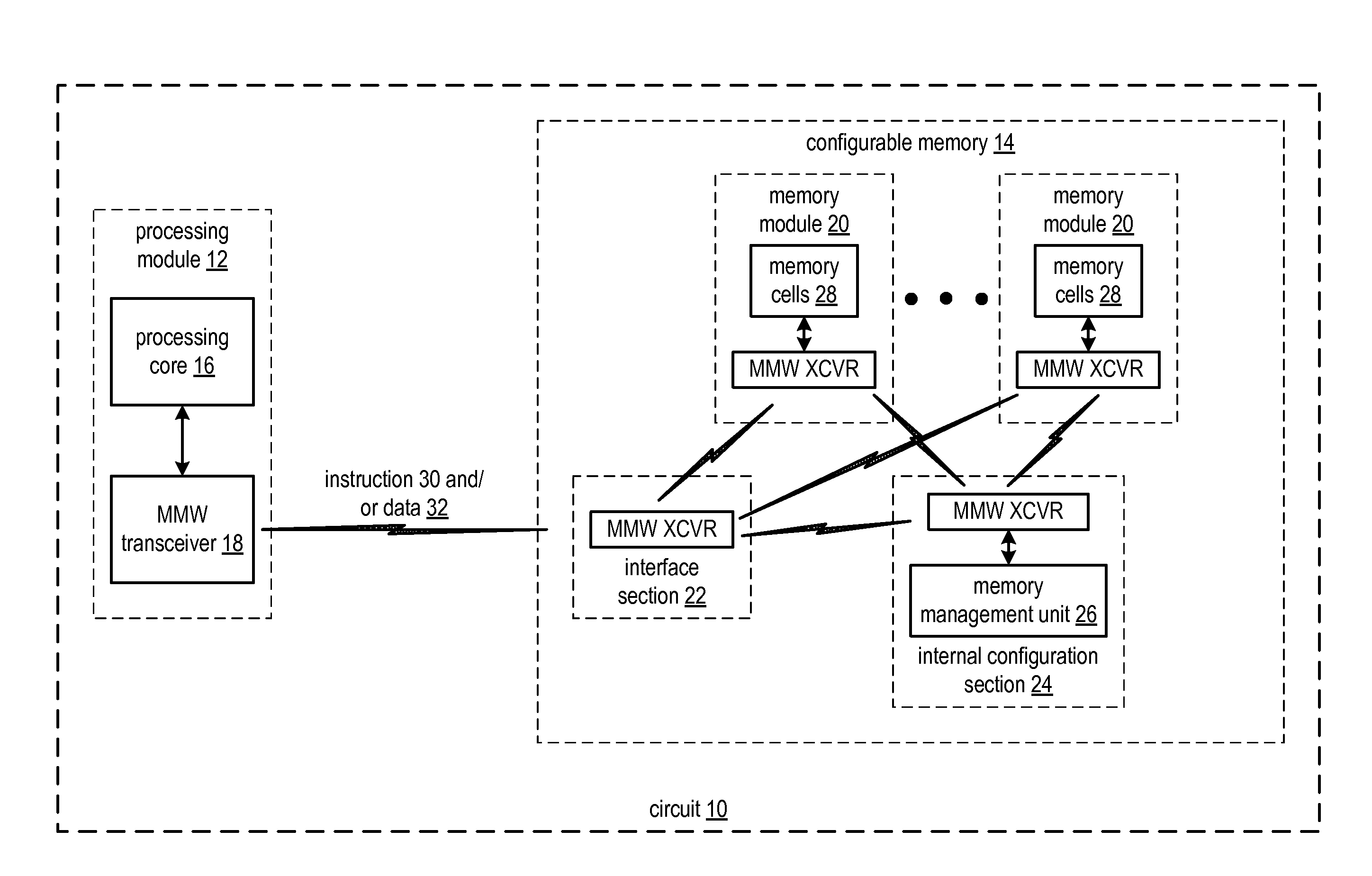
[0031]FIG. 1 is a schematic block diagram of an embodiment of a circuit 10 that includes a processing module 12 and configurable memory 14. The circuit 10 may be implemented as single integrated circuit (IC) including the processing module 12 and the configurable memory 14. Alternatively, the circuit may be implemented as two ICs: one for the processing module 12 and another for the configurable memory 14.

[0032]The processing module 12 includes a processing core 16 and a millimeter wave (MMW) transceiver 18. The processing core 16 may be a single processing device or a plurality of processing devices. Such a processing device may be a microprocessor, micro-controller, digital signal processor, microcomputer, central processing unit, field programmable gate array, programmable logic device, state machine, logic circuitry, analog circuitry, digital circuitry, and / or any device that manipulates signals (analog and / or digital) based on hard coding of the circuitry and / or operational ins...


PUM


Abstract

A configurable memory includes an interface section, a plurality of memory modules, and an internal configuration section. The interface section includes a millimeter wave (MMW) transceiver and interfaces with one or more external components. Each the plurality of memory modules includes a memory MMW transceiver and a plurality of memory cells. The internal configuration section includes a memory management unit and a memory management MMW transceiver. The memory management unit is operable to determine configuration of at least some of the plurality of memory modules to form a memory block, identify an interface MMW transceiver to provide a wireless link to the memory block, and generate a configuration signal based on the determined configuration and the identified interface MMW transceiver. The memory management MMW transmits the MMW configuration signal to the identified interface MMW transceiver and the MMW transceivers of the memory modules.

Description

[0001]This patent application is claiming priority under 35 USC § 120 as a continuation in part patent application of co-pending patent applications:1. entitled COMPUTING DEVICE WITH HANDHELD AND EXTENDED COMPUTING UNITS, having a filing date of Feb. 6, 2008, and a Ser. No. 12 / 026,681;2. RF BUS CONTROLLER, having a filing date of Jan. 31, 2007, and a Ser. No. 11 / 700,285; and3. entitled FLASH MEMORY WITH MILLIMETER WAVE HOST INTERFACE AND METHOD FOR USE THEREWITH, having a filing date of Jul. 31, 2007, and a Ser. No. 11 / 888,068.STATEMENT REGARDING FEDERALLY SPONSORED RESEARCH OR DEVELOPMENT[0002]NOT APPLICABLEINCORPORATION-BY-REFERENCE OF MATERIAL SUBMITTED ON A COMPACT DISC[0003]NOT APPLICABLEBACKGROUND OF THE INVENTION[0004]1. Technical Field of the Invention[0005]This invention relates generally to computing devices and more particularly to components of such computing devices.[0006]2. Description of Related Art[0007]Communication systems are known to support wireless and wire lin...

Claims


Application Information

Patent Timeline
IPC IPC(8): G06F12/00H04M1/72409H04M1/72412
CPCG03G15/6508G03G15/6558G06F1/1632G06F12/0223Y02D10/13G11C5/04G11C7/20H04M1/72527G06F12/0646Y02D10/00H04M1/72412
InventorMARKISON, TIMOTHY W.
OwnerAVAGO TECH INT SALES PTE LTD