

Reducing Resistance in Source and Drain Regions of FinFETs
a technology of finfets and drain regions, which is applied in the direction of semiconductor devices, electrical devices, transistors, etc., can solve the problems of increased gate width, conflict with the requirements of reducing the size of semiconductor devices, and the drawbacks of finfets, so as to reduce the cost of more chip areas, the effect of enlarging the source/drain region of finfets
- Summary
- Abstract
- Description
- Claims
- Application Information
AI Technical Summary
Benefits of technology
Problems solved by technology
Method used
Image

Examples
Embodiment Construction
[0015]The making and using of the presently preferred embodiments are discussed in detail below. It should be appreciated, however, that the present invention provides many applicable inventive concepts that can be embodied in a wide variety of specific contexts. The specific embodiments discussed are merely illustrative of specific ways to make and use the invention, and do not limit the scope of the invention.
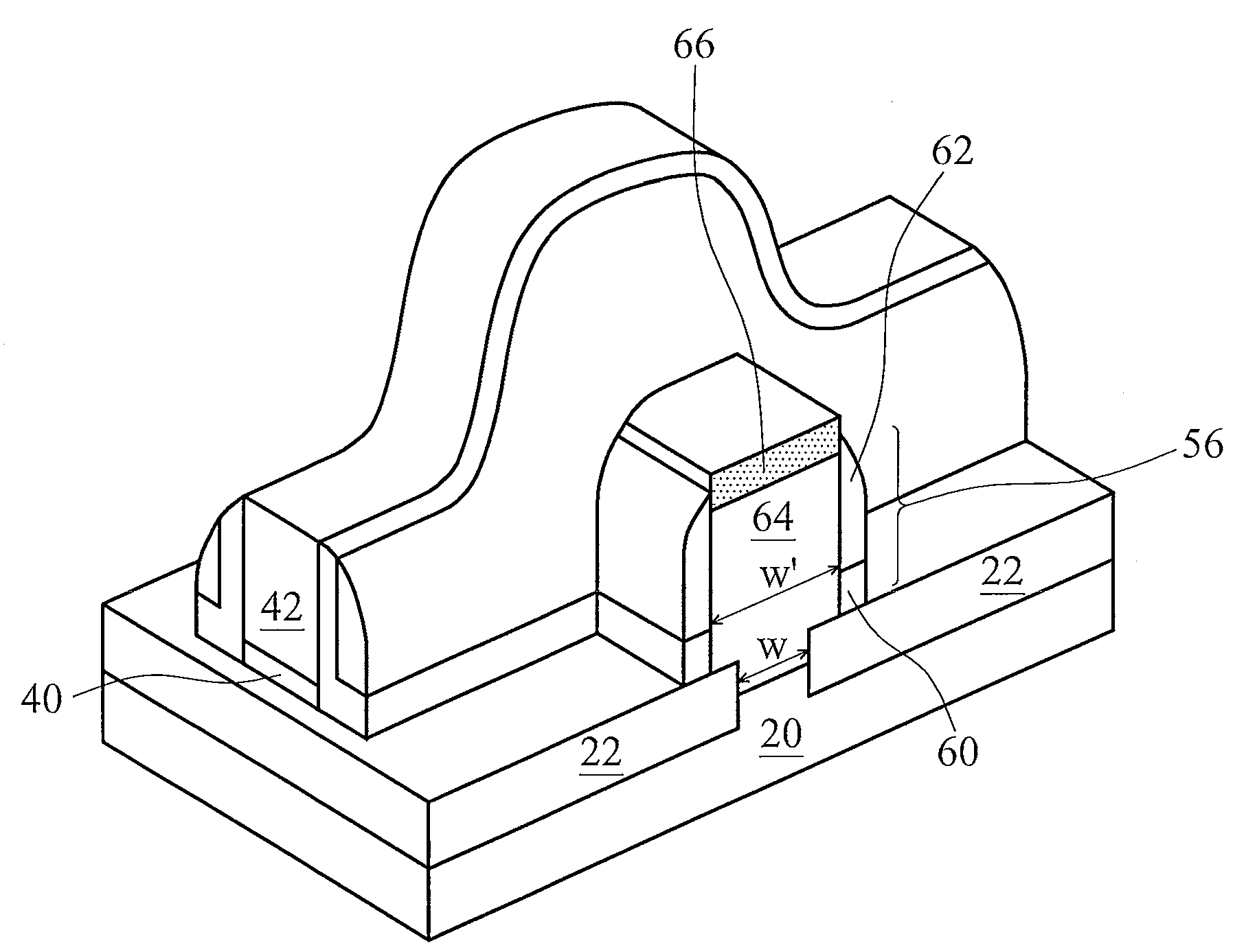
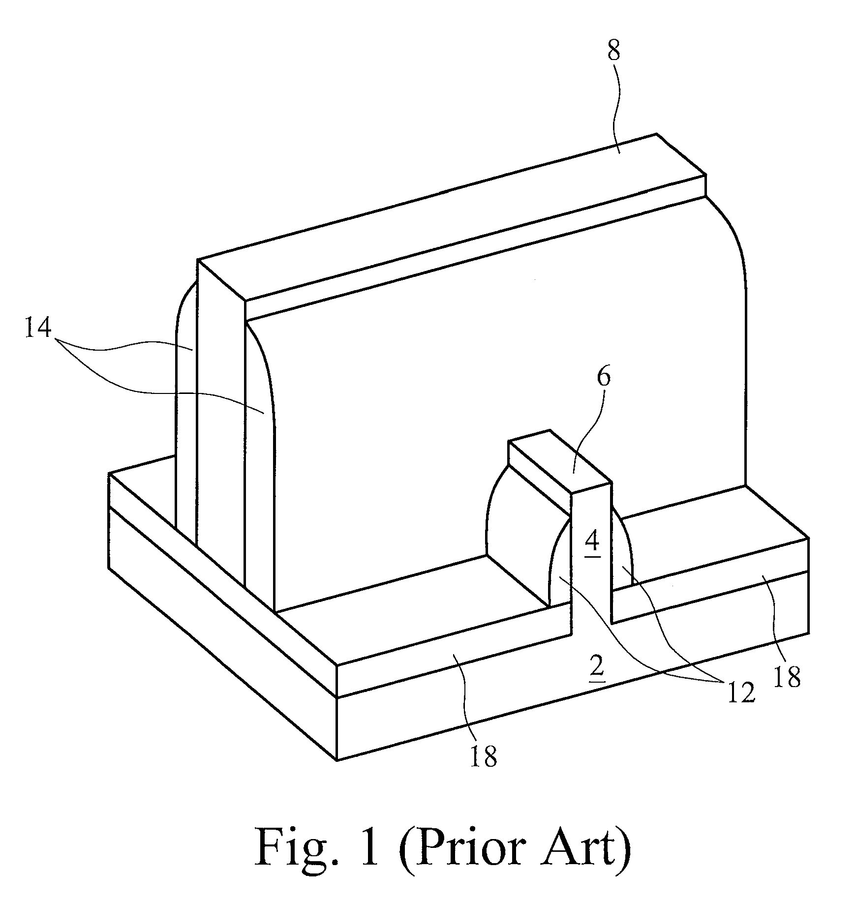
[0016]A novel fin field-effect transistor (FinFET) and the method of forming the same are presented. The intermediate stages of manufacturing a preferred embodiment of the present invention are illustrated. The variations of the preferred embodiments are then discussed. Throughout the various views and illustrative embodiments of the present invention, like reference numbers are used to designate like elements.
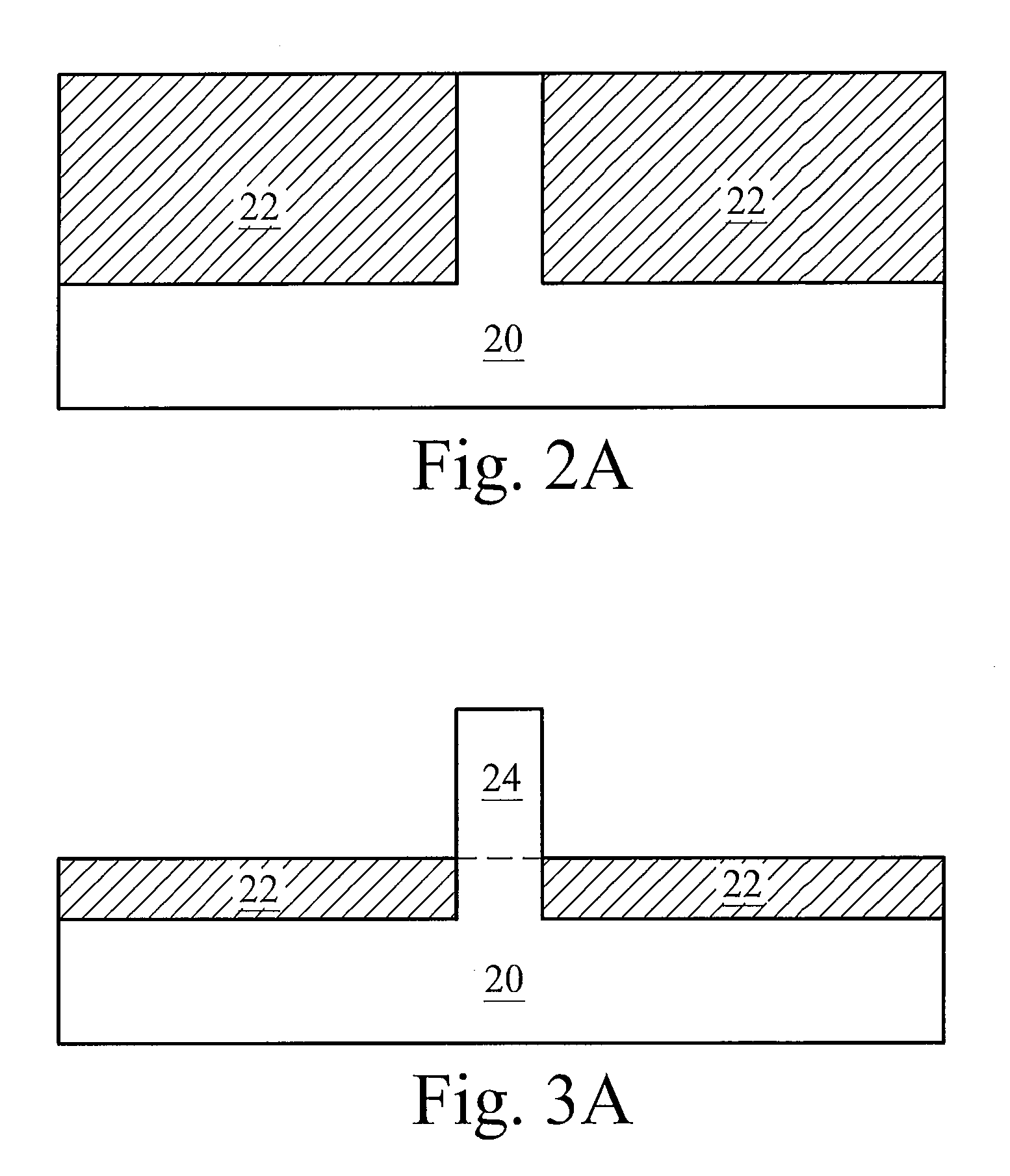
[0017]Referring to FIG. 2A, semiconductor substrate 20 is provided. Semiconductor substrate 20 may be a bulk silicon substrate, a bulk silicon-germanium substrate, or m...
PUM
 Abstract
Description
Claims
Application Information