Addressing schemes for electronic displays

a technology of electronic displays and address schemes, applied in the direction of instruments, optics, static indicating devices, etc., can solve the problems of preventing their widespread use, inadequate service life of these displays, and normally precluding the use of passive matrix addressing methods

Inactive Publication Date: 2009-07-09
E INK CORPORATION
View PDF104 Cites 337 Cited by
  • Summary
  • Abstract
  • Description
  • Claims
  • Application Information

AI Technical Summary

Problems solved by technology

Nevertheless, problems with the long-term image quality of these displays have prevented their widespread usage.
For example, particles that make up electrophoretic displays tend to settle, resulting in inadequate service-life for these displays.
This normally precludes the use of passive matrix addressing methods.
One problem with such high resolution displays is the sheer number of drivers required.
Especially in small displays, the cost of the drivers rivals or may outweigh the cost of the electro-optic material.
Another problem with such high resolution displays is the time taken to address the display.
If the addressing scheme used requires that each row be addressed for the time necessary to completely address an electrophoretic medium (which is typically of the order of 100 milliseconds), the total time taken to address the display may be undesirably great.

Method used


Image

  • Addressing schemes for electronic displays
  • Addressing schemes for electronic displays
  • Addressing schemes for electronic displays

Examples


Embodiment Construction

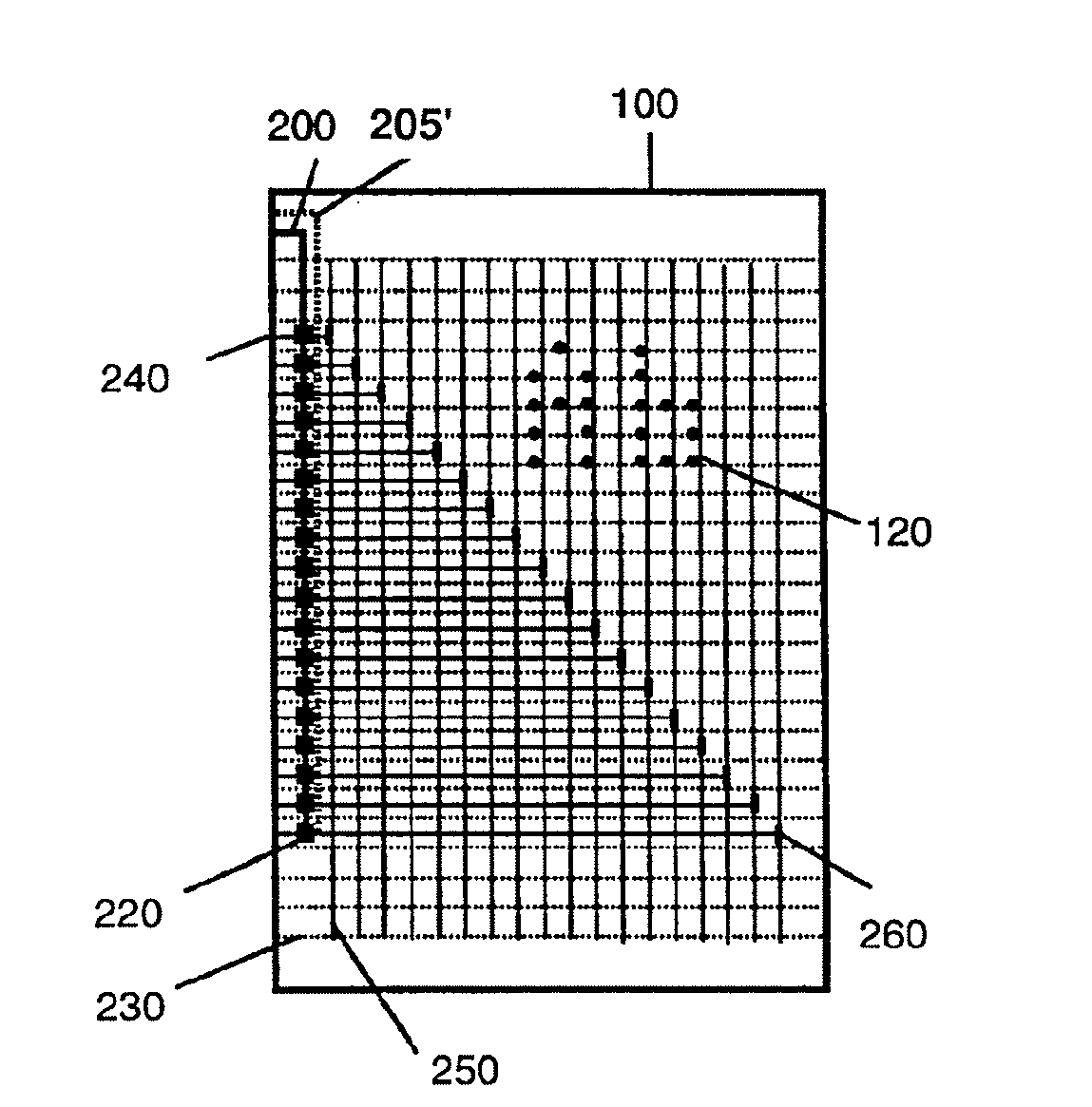
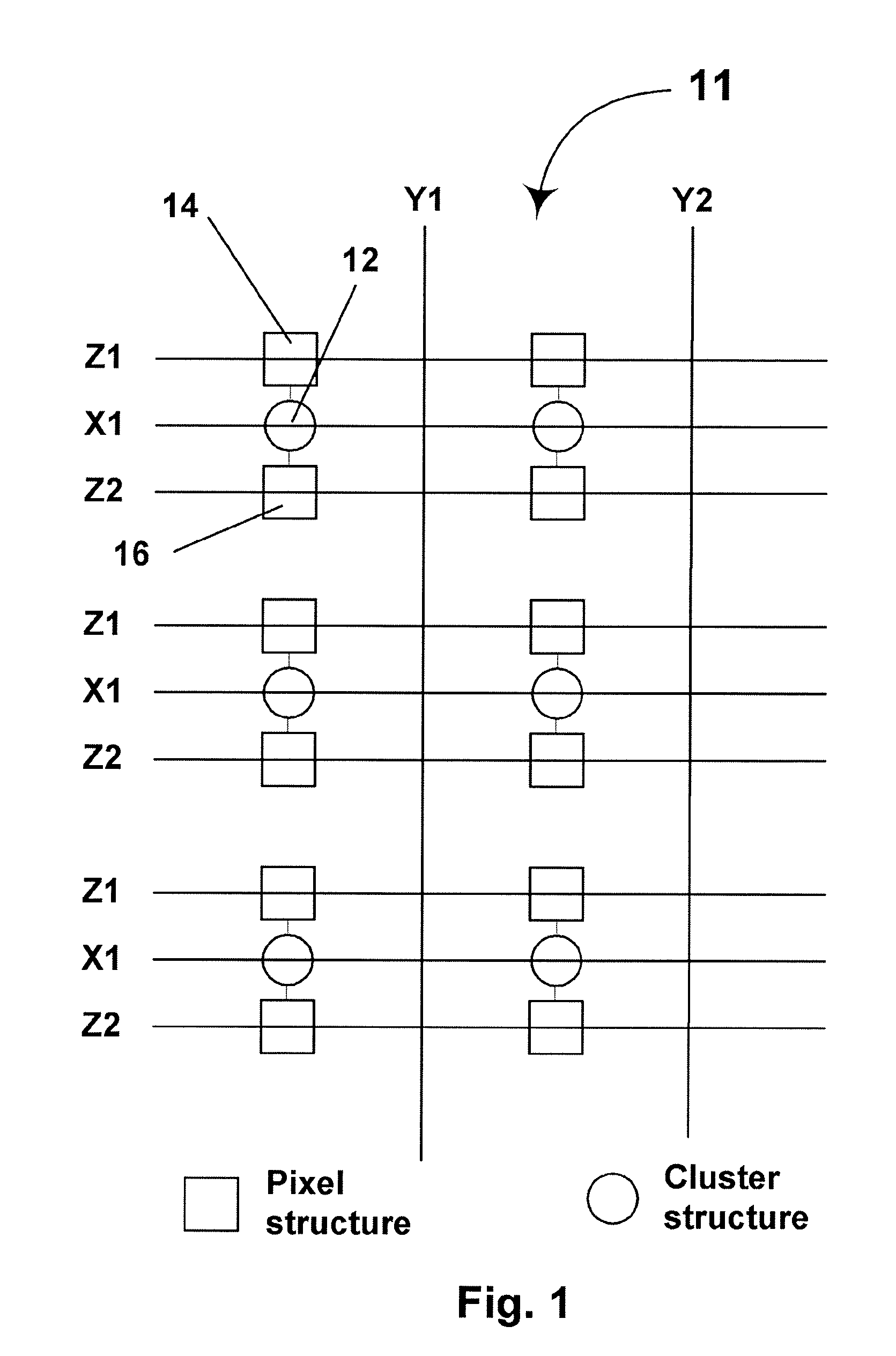
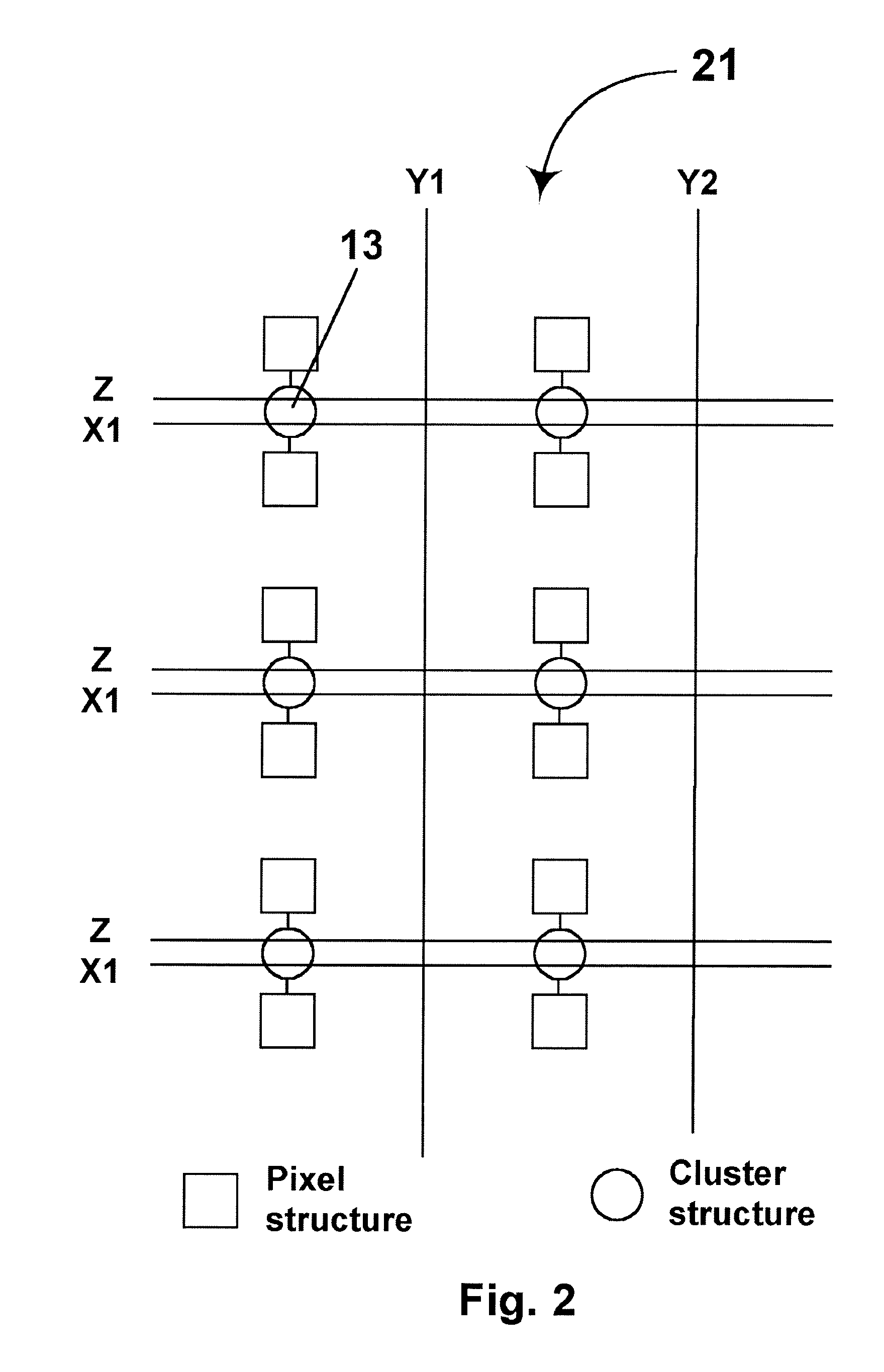
[0069]As already mentioned, the three dimensional displays and methods of the present invention use an electro-optic material having a plurality of pixels, and separate first, second and third sets of addressing means for addressing the pixels. In this display and method, each of the pixels is associated with one addressing means in each of the three sets, such that addressing of any specific pixel requires application of signals within predetermined ranges to each of the three addressing means associated with that specific pixel. The additional dimension is accomplished by introducing a method of addressing sub-arrays within the array. By thus substituting a three-dimensional addressing scheme for a two-dimensional one, the number of drivers can be greatly reduced. In effect, the present invention splits the display into z regions, each addressable by the x columns and y rows, enabling the entire display of x*y*z pixels to be addressed by x+y+z drivers. For example, the aforementio...


PUM

PropertyMeasurementUnit
timeaaaaaaaaaa
electrophoreticaaaaaaaaaa
optical characteristicaaaaaaaaaa

Abstract

An electronic display comprises an electro-optic material (preferably an electrophoretic medium) having a plurality of pixels, and separate first, second and third sets of addressing means for addressing these pixels. Each of the pixels is associated with one addressing means in each of the three sets, such that addressing of any specific pixel requires application of signals within predetermined ranges to each of the three addressing means associated with the specific pixel being addressed. The display may be in the form of a multi-page electronic book.

Description

REFERENCE TO RELATED APPLICATIONS[0001]This application is a divisional of copending application Ser. No. 10 / 906,019, filed Jan. 31, 2005 (Publication No. 2006 / 0139308), which is a continuation-in-part of application Ser. No. 09 / 683,179, filed Nov. 29, 2001 (now U.S. Pat. No. 7,023,420, issued Apr. 4, 2006), which itself claims benefit of Provisional Application Ser. No. 60 / 253,892 filed Nov. 29, 2000. Application Ser. No. 10 / 906,019 is also a continuation-in-part of application Ser. No. 08 / 983,404, filed Jul. 19, 1996 (now U.S. Pat. No. 7,106,296, issued Sep. 12, 2006), which is the U.S. national phase of International Application PCT / US96 / 12000 (Publication No. WO 97 / 04398), filed Jul. 19, 1996, which in turn is (as regards the United States of America) a continuation-in-part of application Ser. No. 08 / 504,896, filed Jul. 29, 1995 (now U.S. Pat. No. 6,124,851, issued Sep. 26, 2000).[0002]The entire disclosures of all the aforementioned applications, and of all U.S. patents and pub...

Claims


Application Information

Patent Timeline
Patent Type & Authority Applications(United States)
IPC IPC(8): G09G3/34
CPCG02F1/1334G09G2360/16G02F2001/1676G02F2201/12G09G3/02G09G3/344G09G3/3446G09G2300/08G09G2310/02G09G2310/0213G09G2310/0221G09G2310/0297G09G2310/04G09G2310/061G09G2320/0252G09G2340/16G02F1/167
Inventor JACOBSON, JOSEPH M.COMISKEY, BARRETTWILCOX, RUSSELL J.
Owner E INK CORPORATION
Why Eureka
Try Eureka