

Probe card
a technology of probes and contacts, applied in the field of probe cards, can solve the problems of extremely small distance between neighboring contact pads and extremely small contact pads, and achieve the effect of facilitating horizontal regulation
- Summary
- Abstract
- Description
- Claims
- Application Information
AI Technical Summary
Benefits of technology
Problems solved by technology
Method used
Image

Examples
Embodiment Construction
Exemplary embodiments of the present invention will now be described in detail with reference to the accompanying drawings. The invention may, however, be embodied in many different forms and should not be construed as being limited to the embodiments set forth herein. Rather, these embodiments are provided so that this disclosure will be thorough and complete, and will fully convey the scope of the invention to those skilled in the art. In the drawings, the shapes and dimensions may be exaggerated for clarity, and the same reference numerals will be used throughout to designate the same or like components.
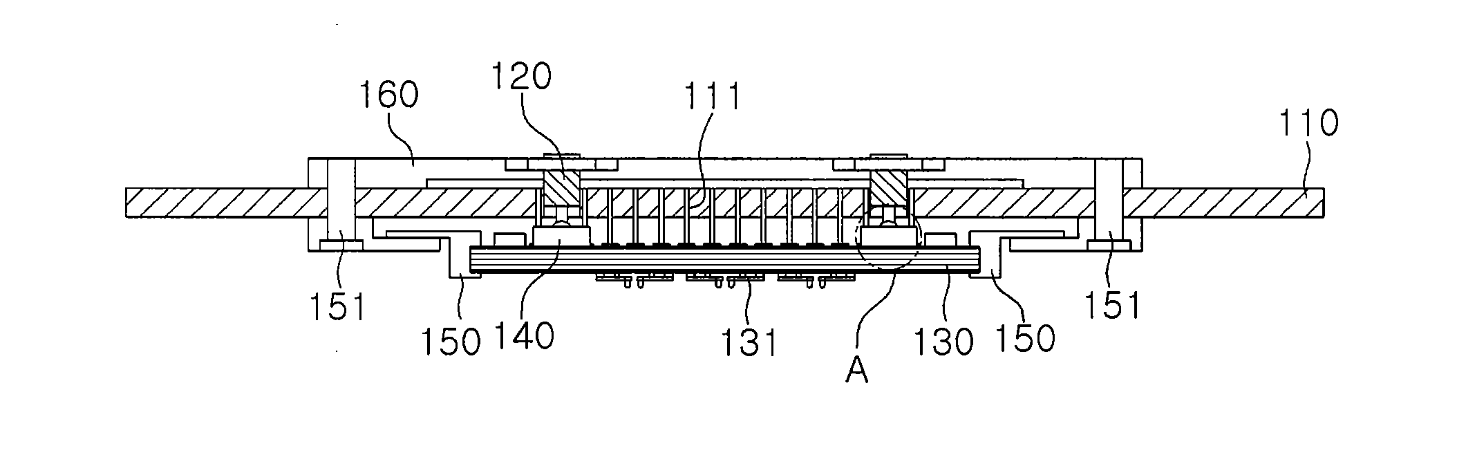
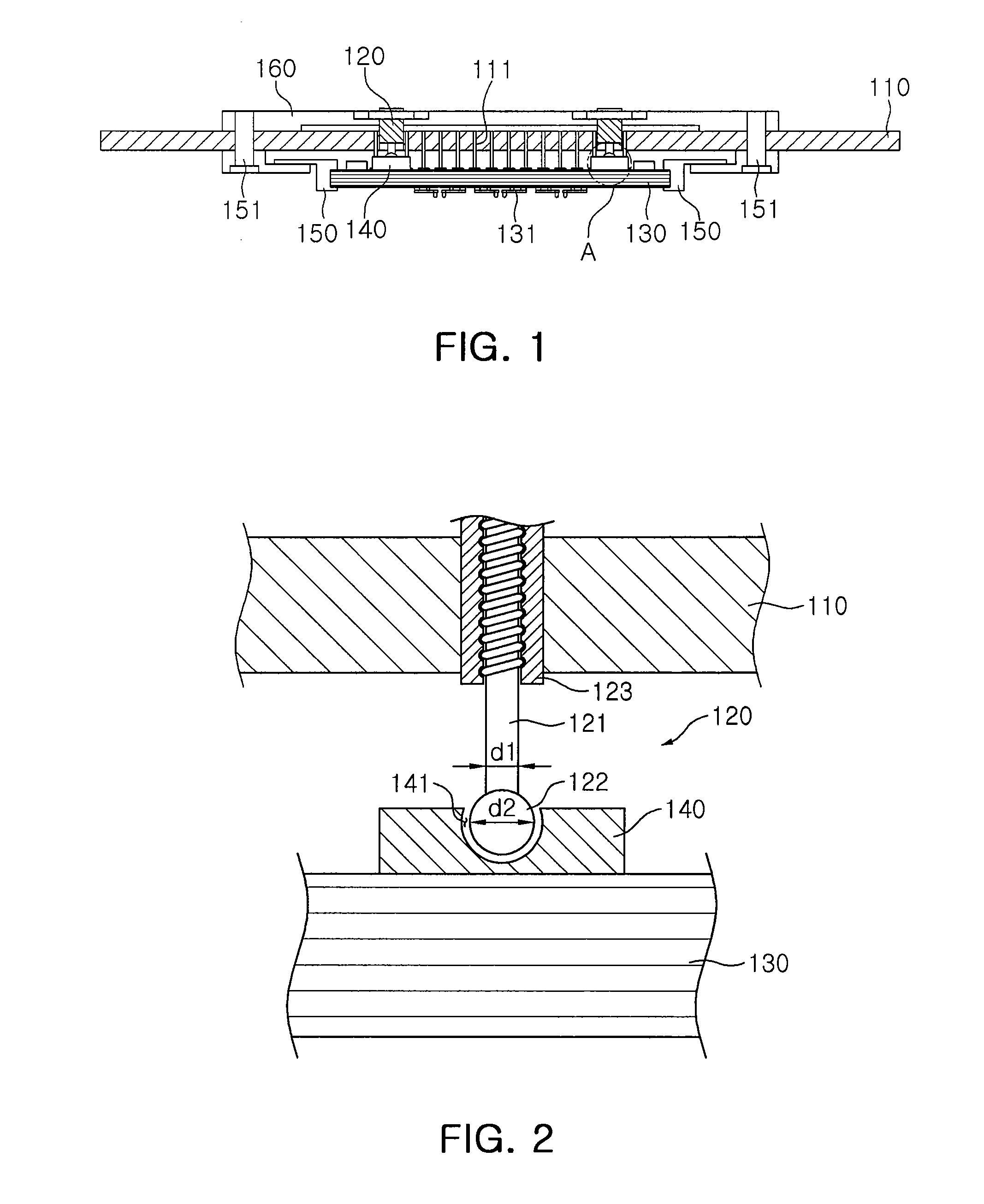
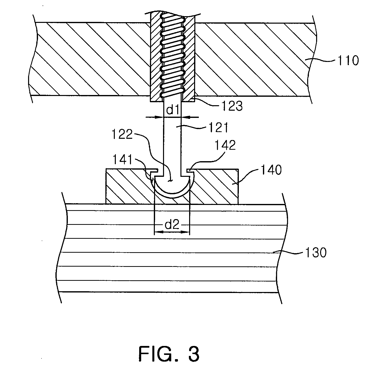
FIG. 1 is a cross-sectional view schematically illustrating a probe card according to an exemplary embodiment of the invention. FIG. 2 is an enlarged sectional view schematically illustrating a region A of FIG. 1.
Referring to FIG. 1, a probe card according to this embodiment includes a printed circuit board 110, horizontal regulators 120, a probe substrate 130, and connection memb...
PUM
 Abstract
Description
Claims
Application Information