

Semiconductor device and method of manufacturing the same
a technology of semiconductor devices and semiconductors, applied in semiconductor devices, semiconductor/solid-state device details, electrical apparatus, etc., can solve the problems of process reappearance and production costs increase, and achieve the effects of simplifying a manufacturing process, reducing the area of a device, and improving reliability
- Summary
- Abstract
- Description
- Claims
- Application Information
AI Technical Summary
Benefits of technology
Problems solved by technology
Method used
Image

Examples
Embodiment Construction
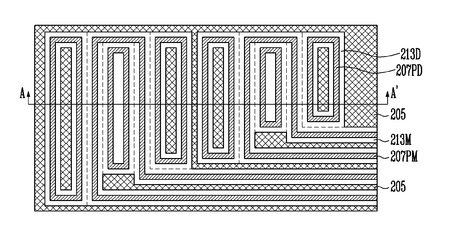
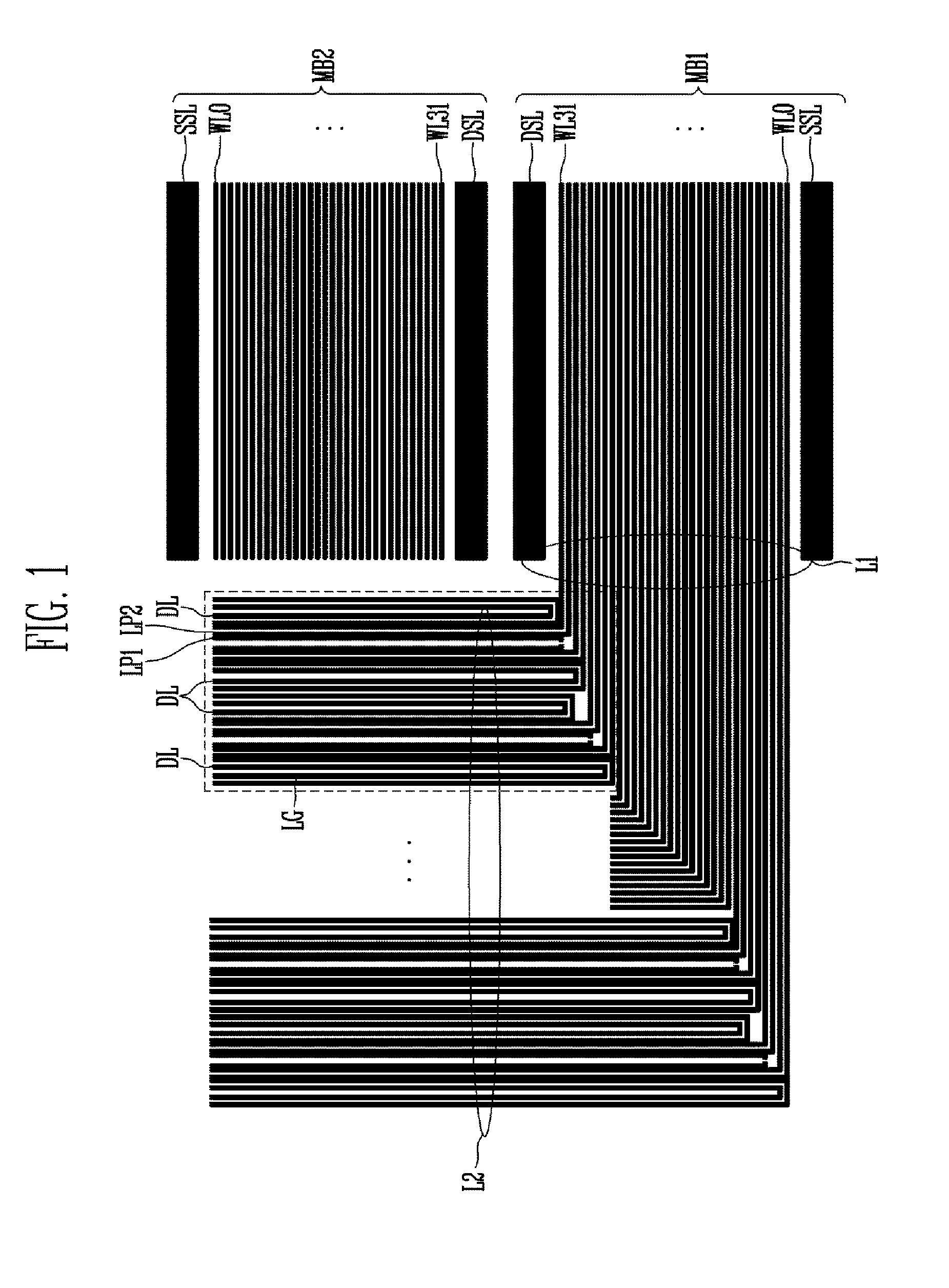
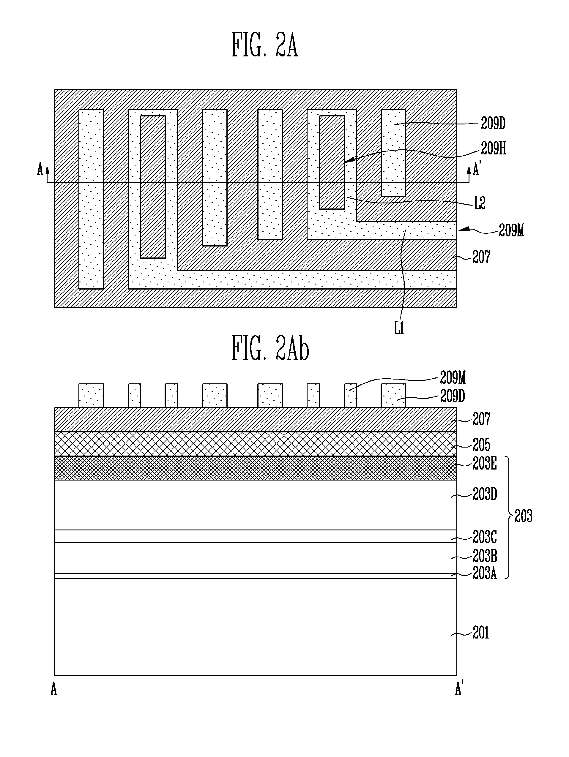
[0014]Hereinafter, various embodiments of the present disclosure will be described in detail with reference to the accompanying drawings. The figures are provided to allow those having ordinary skill in the art to understand the scope of the embodiments of the disclosure. The present invention may, however, be embodied in different forms and should not be construed as limited to the embodiments set forth herein. Rather, these embodiments are provided so that this disclosure will be thorough and complete, and will fully convey the scope of the present invention to those skilled in the art.
[0015]The drawings are not necessarily to scale and in some instances, proportions may have been exaggerated in order to clearly illustrate features of the embodiments. In this specification, specific terms have been used. The terms are used to describe the present invention, and are not used to qualify the sense or limit the scope of the present invention.
[0016]In this specification, ‘and / or’ repre...
PUM
 Abstract
Description
Claims
Application Information