Lateral power device having low specific on-resistance and using high-dielectric constant socket structure and manufacturing method therefor

a technology of specific on-resistance and lateral power device, which is applied in the direction of semiconductor power device, electrical apparatus, basic electric elements, etc., can solve the problems of device specific on-resistance, low permittivity of siosub>2 /sub>, and confined specific on-resistance, etc., to achieve high breakdown voltage, uniform potential distribution, and high permittivity

Active Publication Date: 2015-11-19
UNIV OF ELECTRONICS SCI & TECH OF CHINA
View PDF0 Cites 11 Cited by
  • Summary
  • Abstract
  • Description
  • Claims
  • Application Information

AI Technical Summary

Benefits of technology

[0022]At the off-state of the LJHMOS proposed in this invention, the charge balance and potential modulation effects co-exist because both PN alternating super junction structure and high permittivity material are used in the drift region to guarantee uniform potential distribution and high breakdown voltage. More importantly, because the gate directly contacts the first filler material inside the isolation region, so that the first filler material shares the same potential as the gate; additionally, the potential in the drift region is much lower than the gate. The strong accumulation effect is generated in the drift region at the both sides of isolation region through the high permittivity material sockets. As the result, massive electron charges are absorbed to the interface of the drift region and high permittivity sockets; the carrier density at the drift region is significantly increased with no additional drift region doping; the device specific on-resistance will be reduced in orders of magnitude.
[0023]On the other hand, strong accumulation effect also introduces some negative effects to the performance of the power device. The LJHMOS proposed in this invention exhibits large parasitic capacitor between gate and drain, which causes large switch loss. In actual application, it is advisable to transfer the merit of low specific on-resistance of the LJHMOS to the shrinking of the device size. With such small device specific on-resistance of this invention, the device gains much lower total on-resistance under the same area condition compared with the conventional device; on other hand, the area of the LJHMOS could be much smaller than the conventional device under the condition of the same on-resistance. As the parasitic capacitance always decreases with the shrinking of the device area, when the device is designed with a smaller size, the negative effect caused by parasitic capacitance will be significantly reduced or even eliminated. Therefore, under the condition of similar on-resistance, switch loss, and breakdown voltage, the LJHMOS allows much smaller device area than that of the super junction device. Above all, the advantage of this invention in actual application is that the power device size can be significantly reduced with no decreasing of breakdown voltage and no increasing of specific on-resistance.

Problems solved by technology

Consequently, the device specific on-resistance is confined to meet the RESURF condition for high breakdown voltage.
Although its performance is better than that of the RESURF LDMOS, the conduction of Super Junction still relies on drift region doping; its specific on-resistance is a limited under given breakdown voltage condition.
However, because the permittivity of the SiO2 is very low, the accumulation effect is limited; and the thin SiO2 is also fragile for high voltage.
Furthermore, the low permittivity of the SiO2 may cause the potential gathering, which is negative for high breakdown voltage.

Method used


Image

  • Lateral power device having low specific on-resistance and using high-dielectric constant socket structure and manufacturing method therefor
  • Lateral power device having low specific on-resistance and using high-dielectric constant socket structure and manufacturing method therefor
  • Lateral power device having low specific on-resistance and using high-dielectric constant socket structure and manufacturing method therefor

Examples


embodiment 1

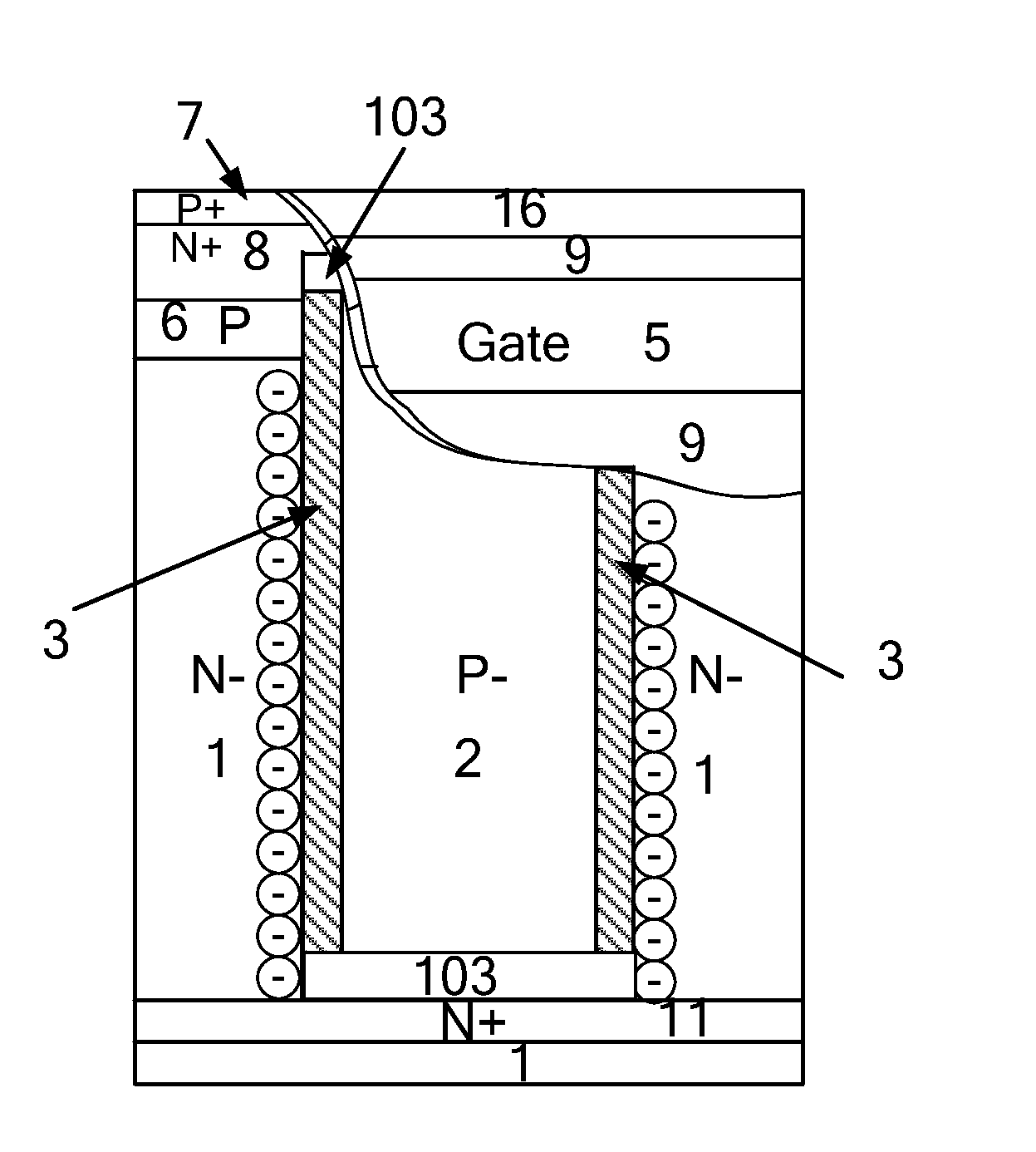
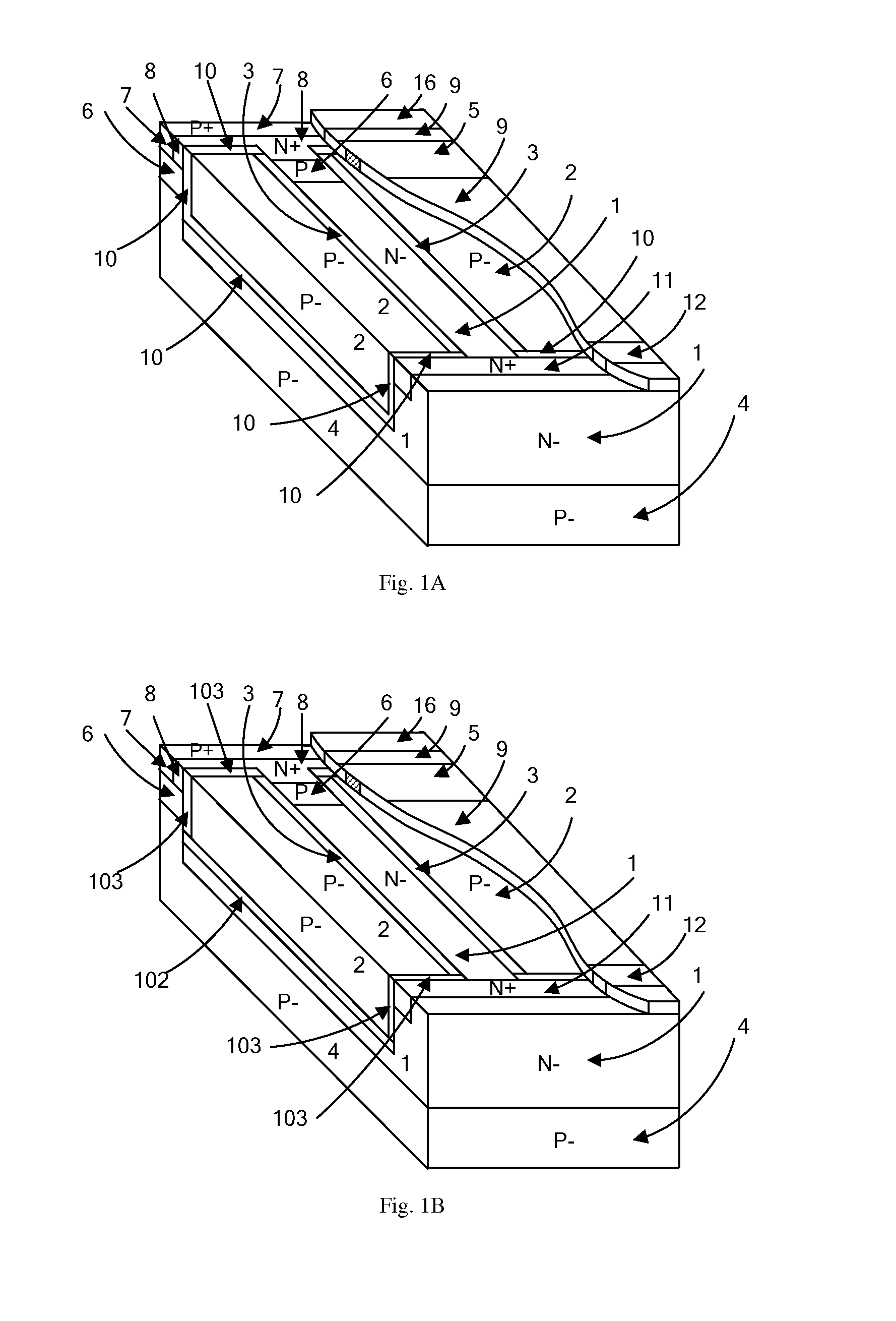
[0048]This embodiment uses the P− doped silicon as the material for substrate 4 and the first filler material 2 inside the isolation region, and uses the N doped conductive type silicon as the drift region 1. Besides, this embodiment 1 also comprises the channel region 6, ohm contact heavy doping region 7, source 8, gate 5, drain 11, drain contact 12, source contact 16, high permittivity material socket 3, the first dielectric layer 10 (including the bottom 102 and end face sidewall 103), and the second dielectric layer 9 using SiO2 or high permittivity material. At least two isolation regions are placed into the drift region 1; the drift region 1 and channel region 6 locate between the adjoining isolation regions; and each isolation extends from source 8 to drain 11; the boundary of isolation regions are formed by high permittivity material socket 3 and the first dielectric layer 10; the bottom 102 of the first dielectric layer 10 locates at the bottom of the first filler material ...

embodiment 2

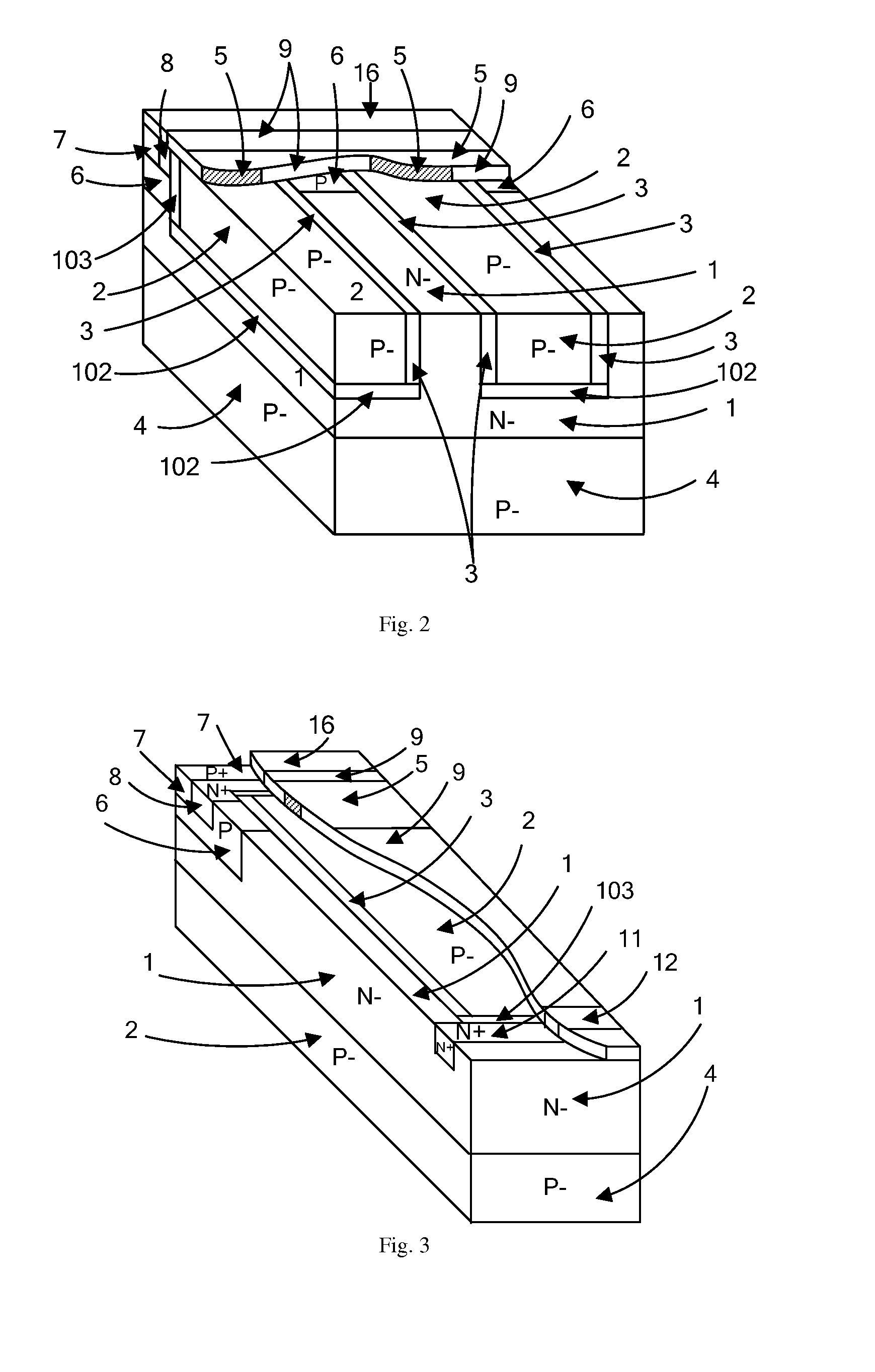
[0051]As shown in FIG. 5-7. This embodiment uses the P− silicon as the substrate 4, and uses the N− silicon as the drift region 1. The isolation regions are partially filled by the third filler material 51 at the side of the source. The third filler material uses the same material as the gate 5, and the gate 5 contacts the third filler material 51 through the via (the shadow part in the FIG. 5) on the second dielectric layer 9, the rest part of the isolations are filled by the first filler material 2, which is the same material as the high permittivity sockets 3. The source contact 16 connects the source 8 and ohm contact heavy doping region 7 through the via on the second dielectric layer 9, the drain 11 contacts drain contact through the via on the second dielectric layer 9.

[0052]Although this embodiment only uses the potential modulation effect of high permittivity to optimize the potential distribution without N&P alternating structure, whereas the high permittivity material tak...

embodiment 3

[0053]The difference between this embodiment and the embodiment 1 is that the material of first filler material 2 is N− silicon for this embodiment. Also, this embodiment uses the P− and N− as the silicon substrate 4 and drift region 1, respectively.

[0054]As the material of the first filler material 2 is not the P− silicon for this embodiment, the potential distribution optimization only relies on the modulation effect of the high permittivity material. However, the proportion of the high permittivity in the drift region is lower than that of the embodiment 2, the average permittivity improvement between drain 11 and source 8 is limited. Consequently, the breakdown voltage of this embodiment is lower than that of the embodiment 1. Although the N− silicon is used as the first filler material inside the isolation region, the N− silicon direct contacts the gate 5 but isolated from drain 11, the strong accumulation effect will happen in the entire drift region at the device on state lik...


PUM

PropertyMeasurementUnit
dielectric constantaaaaaaaaaa

Abstract

Provided is a lateral power device having low specific ON-resistance and using a high-dielectric constant socket structure and a manufacturing method therefor, which relate to semiconductor power devices. A source electrode (8) of the device is of a first conduction type, and a channel region (6), a silicon substrate (4) and an ohmic contact heavily-doped region are of a second conduction type; at least two isolation regions are arranged in an embedded manner in a drift region (1); between the isolation regions are the drift region (1) and the channel region (6); each isolation region extends from the source electrode (8) to a drain electrode (11); high-dielectric constant material strips (3) and first insulation dielectric layers (10) form boundaries of the bottoms and sidewalls of the isolation regions; the isolation regions are filled with a first filling material (2), a second insulation dielectric layer (9) is arranged on the upper surface of the drift region (1) and the upper surfaces of the isolation regions, and a gate electrode (5) directly contacts the first filling material (2) via holes on the second insulation dielectric layer (9); and a source electrode lead-out wire (16) and a drain electrode lead-out wire (12) directly contact the source electrode (8) and the drain electrode (11) respectively via the holes on the second insulation dielectric layer (9). The area of a power device can be greatly reduced on the premise of not reducing the withstand voltage and not increasing the specific ON-resistance.

Description

FIELD OF INVENTION[0001]This invention relates to semiconductor devices, in particular to the material and structure of voltage-sustaining layers for lateral semiconductor power device.BACKGROUND OF THE INVENTION[0002]It is well known that in a conventional lateral power device, the reverse voltage is sustained by a lightly doped semiconductor drift region, such as the Lateral Double Diffused Metal Oxide Semiconductor (LDMOS). If junction depth and doping concentration of drift region meet the RESURF (reduce the device surface field by reinforcing the body field) condition, the drift region will be fully depleted and space charges are introduced. Therefore, the LDMOS is capable of withstanding high voltage at the off-state. The RESURE condition reported by literature [J. A. Appels, M. G. Collet. P. Hart, H. Vaes, J. Verhoeven. Thin-layer HV-devices [J]. Philips Journal of Research, 1980, 35(1):1˜13] is as below:Nepitepi≤2×10¹²NepiPsub+Nepi≤1.4×1012cm-2[0003]The Psub, Nepi, tepi are ...

Claims


Application Information

Patent Timeline
Patent Type & Authority Applications(United States)
IPC IPC(8): H01L29/78H01L29/66
CPCH01L29/7802H01L29/66712H01L29/7812H01L29/405H01L29/407H01L29/7816H01L29/0634H01L29/0653H01L29/408
Inventor LI, JUNHONGLI, PING
Owner UNIV OF ELECTRONICS SCI & TECH OF CHINA
Why Eureka
Try Eureka