

Semiconductor device and method for manufacturing the same
a technology of semiconductor devices and shielding diodes, which is applied in the direction of semiconductor devices, semiconductor/solid-state device details, diodes, etc., can solve the problems of increasing the area of the chip, easy destruction of the mosfet, etc., and achieves the effect of minimizing the planar chip area of the device and simple method for forming the protection diod
- Summary
- Abstract
- Description
- Claims
- Application Information
AI Technical Summary
Benefits of technology
Problems solved by technology
Method used
Image

Examples
first embodiment
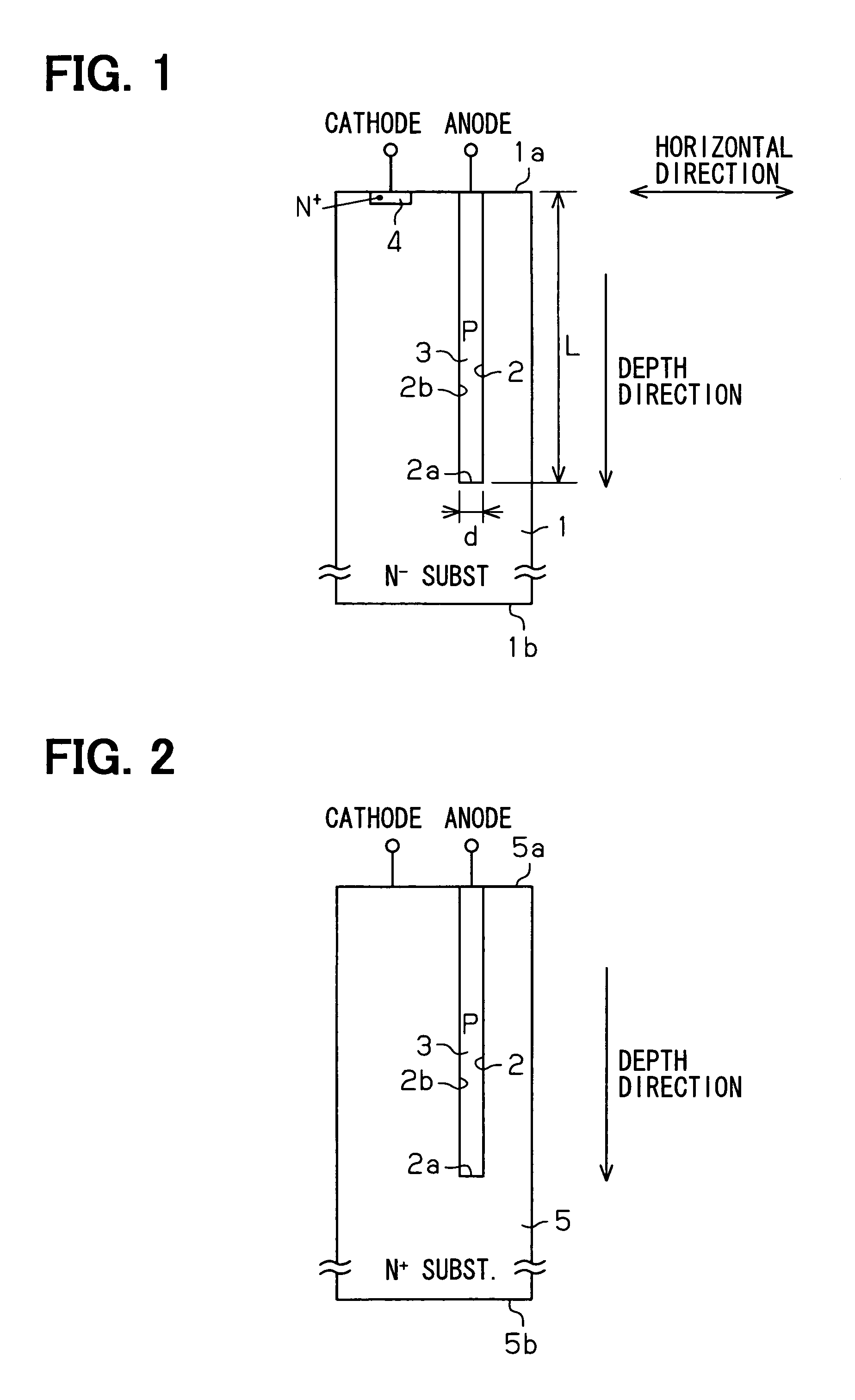
[0046]FIG. 1 shows a longitudinal sectional view of a semiconductor device according to a first embodiment of the present invention. The semiconductor device corresponds to a protection diode, and has been manufactured in a substrate. This protection diode is employed in order to protect an element which has been formed in the same substrate as that of the protection diode, or to protect an element formed in another chip in order that these elements may not be destroyed by a surge current caused by static electric energy and inverse electromotive force of an inductive load.
[0047]While an N− type silicon substrate 1 functioning as a first conductivity type semiconductor substrate owns a major front surface 1a and a rear surface 1b, a diode has been manufactured in the N− type silicon substrate 1. Concentration of the N− type silicon substrate 1 is 1×10¹⁴ to 1×1018 cm−3.
[0048]A trench (diode forming-purpose trench) 2 has been formed in the major front surface 1a of the N− type silicon...
second embodiment
[0058]Next, a difference between the first embodiment and a second embodiment will be mainly explained.
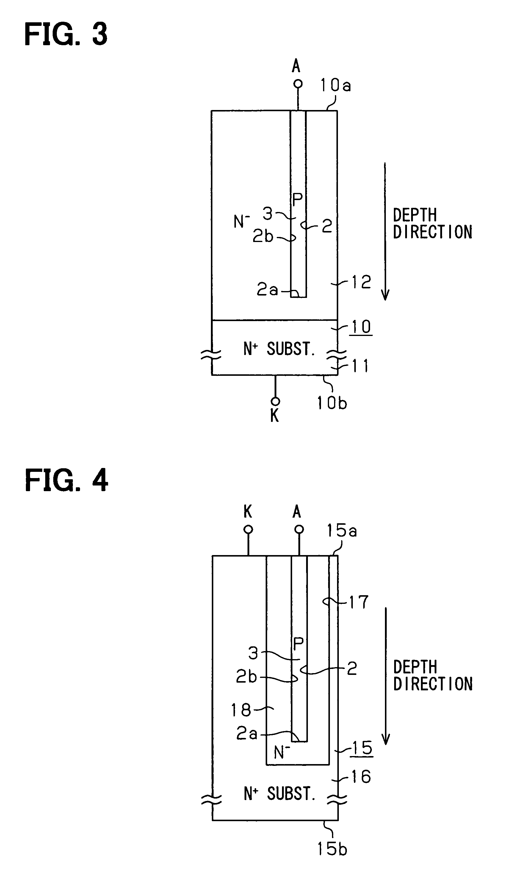
[0059]FIG. 3 shows a longitudinal sectional view of a semiconductor device according to this second embodiment.
[0060]A different point from the first embodiment is given as follows: That is, as a semiconductor substrate (N type substrate) 10 functioning as a first conductivity type semiconductor substrate, an N+ / N− epitaxial substrate is employed in which an N− type silicon layer (first conductivity type epitaxial film having low concentration) 12 has been formed on an N+ type silicon substrate 11 (first conductivity type substrate having high concentration). The semiconductor substrate (N type substrate) 10 owns a major front surface 10a and a rear surface 10b.
[0061]In the N− type silicon layer (first conductivity type epitaxial film having low concentration) 12, a trench 2 has been elongated from the major front surface 10a (upper plane of N− type silicon layer 12) of the semico...
third embodiment
[0071]Next, a third embodiment will now be described by mainly explaining a different point from that of the first and second embodiments.
[0072]FIG. 5 shows a longitudinal sectional view of a semiconductor device according to this third embodiment.
[0073]The technical different point from that of the first and second embodiments is given as follows: That is, a bottom portion of a P type silicon layer 3 is made in a round shape, namely made of a rounded structure.
[0074]In FIG. 5, the bottom portion 3a of the P type silicon layer 3 of FIG. 1 has been rounded. In other words, a bottom plane 2a of a trench 2 has been made round, and the bottom portion 3a of the P type silicon layer (second conductivity type semiconductor layer) 3 has been rounded. As a result, it is possible to suppress lowering of a withstanding voltage which is caused by concentration of electric fields in the bottom portion, so that a low resistance diode having a small area and a high withstanding voltage can be real...
PUM
 Abstract
Description
Claims
Application Information