

Structure of a lateral diffusion MOS transistor in widespread use as a power control device
a technology of lateral diffusion mos and transistor, which is applied in the direction of transistors, semiconductor devices, electrical equipment, etc., can solve the problems of large area still required, limitation of power control system downsizing, etc., and achieve the effect of reducing the device area on a plane, and reducing the size of the lateral diffusion mos
- Summary
- Abstract
- Description
- Claims
- Application Information
AI Technical Summary
Benefits of technology
Problems solved by technology
Method used
Image

Examples
first embodiment
[0029]Preferred embodiments of the invention are described in detail hereinafter with reference to the accompanying drawings. In the present specification and the accompanying drawings, constituents having substantially the same function and constitution are denoted by like reference numerals, thereby omitting duplicated description. First Embodiment
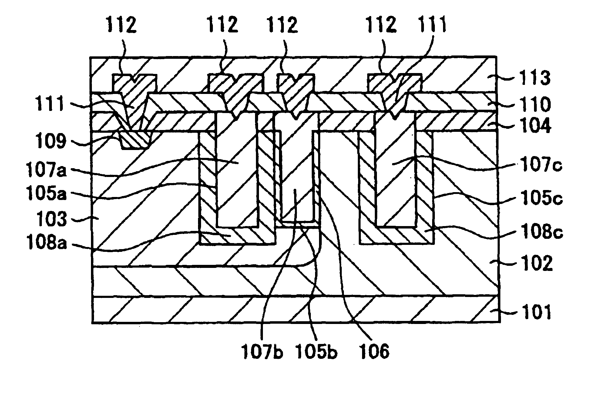
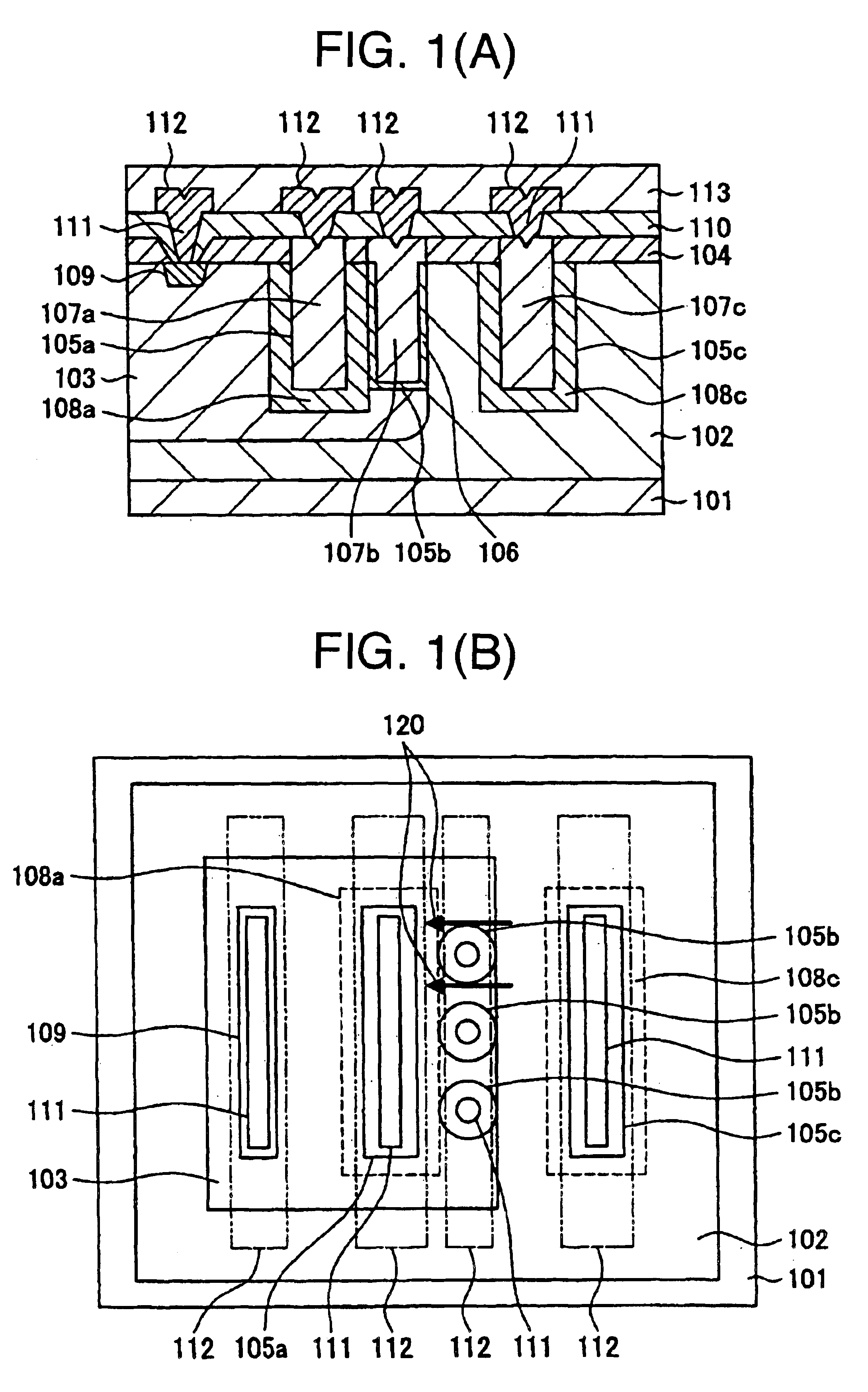
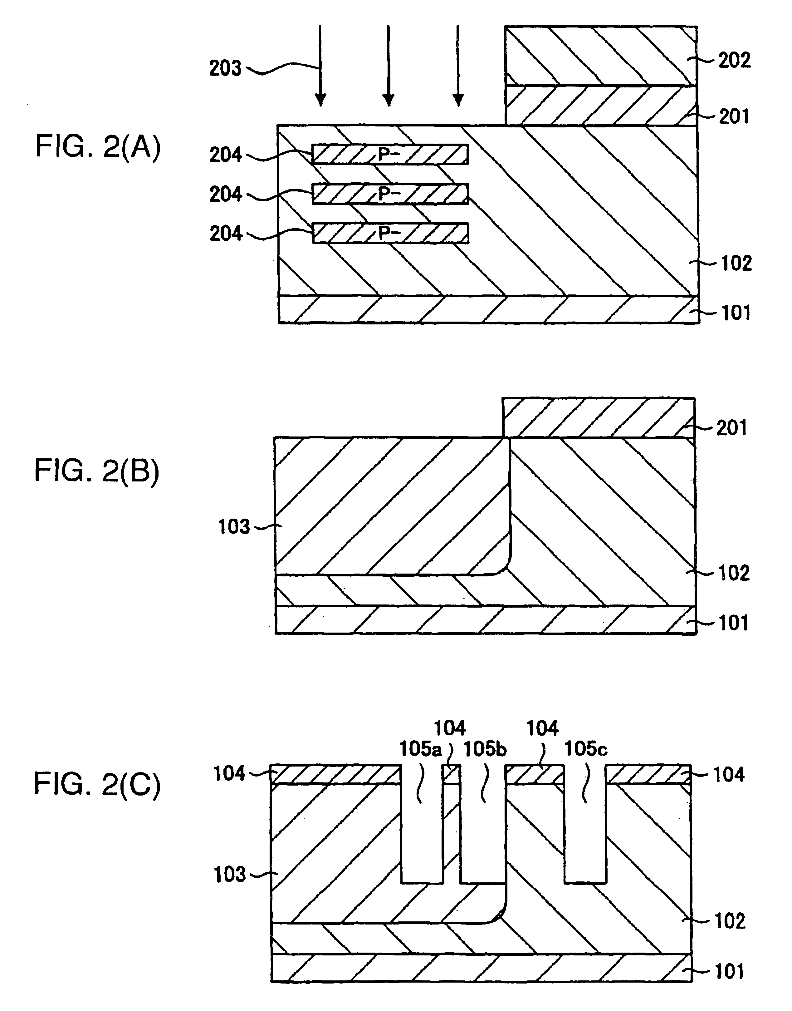
[0030]FIG. 1 (a) is a sectional view illustrating a trench type LDMOS, that is, a first embodiment of a semiconductor device according to the invention. With the present embodiment, an NMOS is described as an example. The trench type LDMOS comprises an N well layer 102 of a second conductivity type, formed on a p-type semiconductor substrate 101, that is, a substrate of a first conductivity type, a P well layer 103 of the first conductivity type, formed in the N well layer 102, a source electrode 107a, a gate electrode 107b, formed in a source trench cavity 105a, a gate trench cavity 105b, respectively, within the P well layer 103, and a...
PUM
 Abstract
Description
Claims
Application Information