Semiconductor device and display device including semiconductor device

a technology of semiconductor devices and display devices, which is applied in the direction of semiconductor devices, electrical devices, transistors, etc., can solve the problems of adversely affecting the characteristics of transistors, image quality degradation of display devices, and electrical characteristics of different transistors, so as to achieve low manufacturing costs, signal delay, and relatively simple manufacturing process

Active Publication Date: 2016-11-24
SEMICON ENERGY LAB CO LTD
View PDF0 Cites 144 Cited by
  • Summary
  • Abstract
  • Description
  • Claims
  • Application Information

AI Technical Summary

Benefits of technology

[0009]As examples of a transistor including an oxide semiconductor film, an inverted staggered transistor (also referred to as a transistor having a bottom-gate structure), a staggered transistor (also referred to as a transistor having a top-gate structure), and the like are given. In the case where a transistor including an oxide semiconductor film is used for a display device, an inverted staggered transistor is used more often than a staggered transistor because a manufacturing process thereof is relatively simple and manufacturing cost thereof can be kept low. However, signal delay or the like is increased by parasitic capacitance that exists between a gate electrode and source and drain electrodes

Problems solved by technology

However, signal delay or the like is increased by parasitic capacitance that exists between a gate electrode and source and drain electrodes of an inverted staggered transistor and accordingly image quality of a display device degrades, which has posed a problem, as an increase in screen size of a display device proceeds, or a display device is provided with a higher resolution image (e.g., a high-resolution display device typified by 4K×2K pixels (3840 pixels in the horizontal direction and

Method used


Image

  • Semiconductor device and display device including semiconductor device
  • Semiconductor device and display device including semiconductor device
  • Semiconductor device and display device including semiconductor device

Examples


embodiment 1

[0082]In this embodiment, examples of a semiconductor device including a transistor and a method for manufacturing the semiconductor device are described with reference to FIGS. 1A to 1C, FIGS. 2A to 2C, FIGS. 3A to 3C, FIGS. 4A to 4C, FIGS. 5A to 5C, FIGS. 6A to 6C, FIGS. 7A and 7B, FIGS. 8A and 8B, FIGS. 9A and 9B, FIGS. 10A and 10B, FIGS. 11A and 11B, FIGS. 12A and 12B, FIGS. 13A to 13D, FIGS. 14A to 14D, FIGS. 15A to 15C, FIGS. 16A to 16D, FIGS. 17A to 17D, FIGS. 18A to 18D, and FIGS. 19A and 19B.

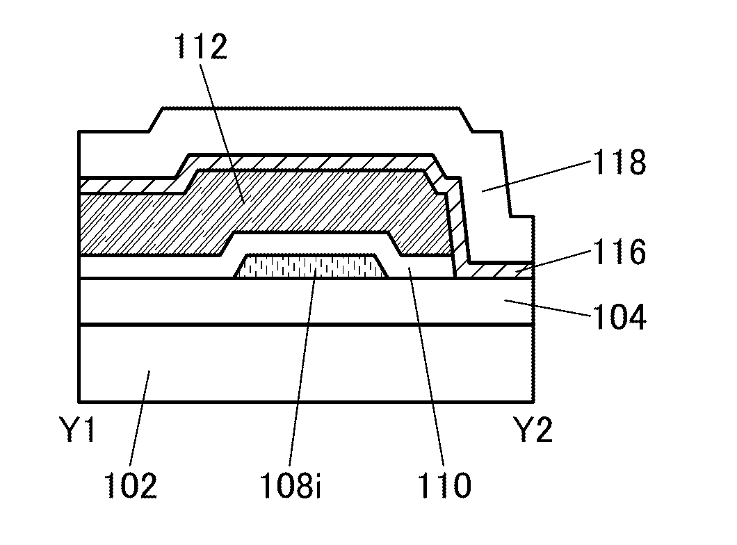
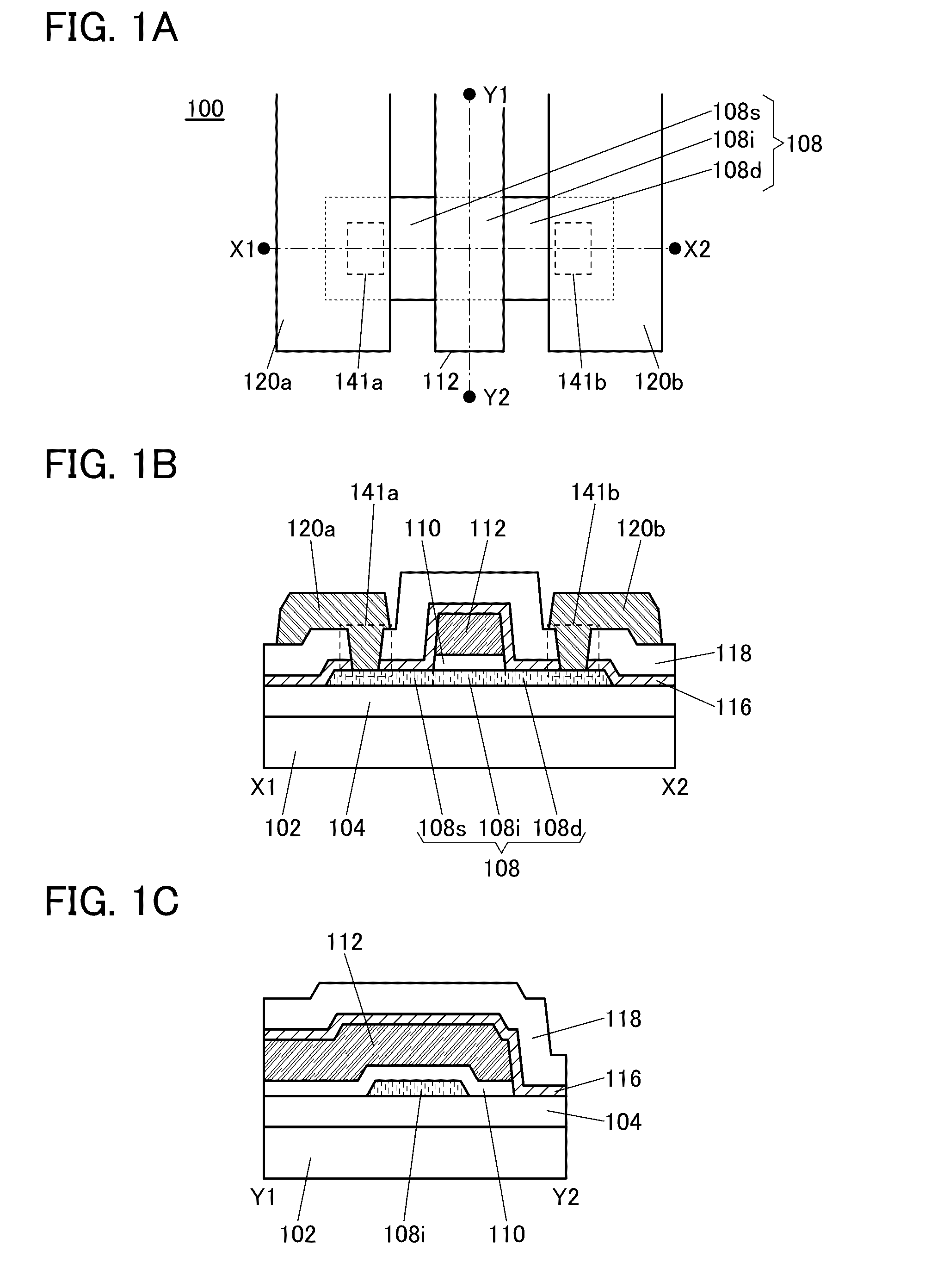
[0083]FIGS. 1A to 1C illustrate an example of a semiconductor device including a transistor. Note that the transistor illustrated in FIGS. 1A to 1C has a top-gate structure.

[0084]FIG. 1A is a top view of a transistor 100. FIG. 1B is a cross-sectional view taken along the dashed-dotted line X1-X2 in FIG. 1A. FIG. 1C is a cross-sectional view taken along the dashed-dotted line Y1-Y2 in FIG. 1A. Note that in FIG. 1A, components such as an insulating film 110 are omitted for clarity. In a m...

modification example 1

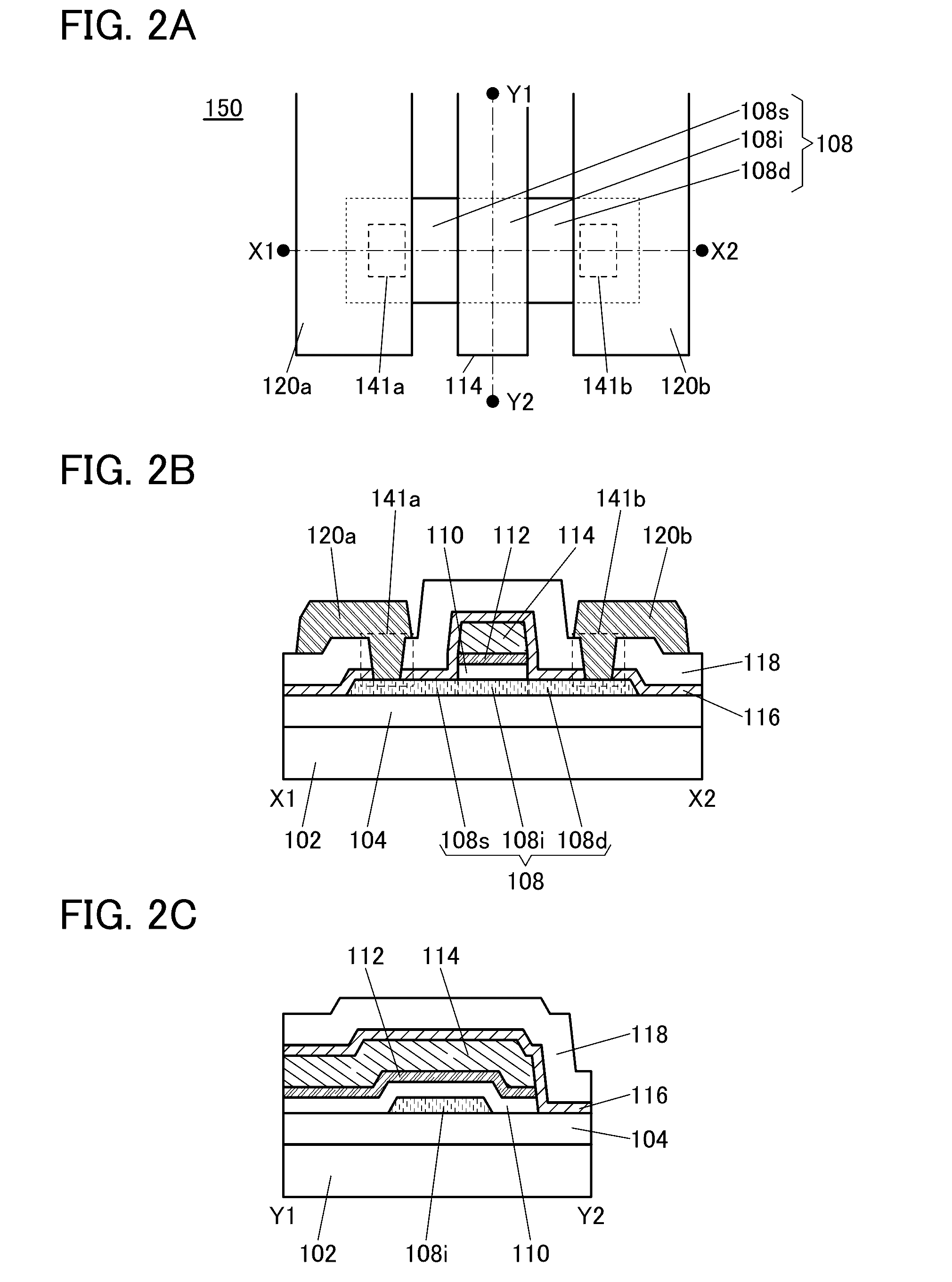
[0172]Next, a modification example of the semiconductor device in FIGS. 3A to 3C is described with reference to FIGS. 7A and 7B.

[0173]FIGS. 7A and 7B are cross-sectional views of a transistor 100C. A top view of the transistor 100C is similar to that of the transistor 100B in FIG. 5A and will be described with reference to FIG. 5A. FIG. 7A is a cross-sectional view taken along the dashed-dotted line X1-X2 in FIG. 5A, and FIG. 7B is a cross-sectional view taken along the dashed-dotted line Y1-Y2 in FIG. 5A.

[0174]The transistor 100C is different from the transistor 100B described above in that an insulating film 122 functioning as a planarization insulating film is provided. Note that the other components of the transistor 100C are similar to those of the transistor 100B described above, and an effect similar to that of the transistor 100B can be obtained.

[0175]The insulating film 122 has a function of planarizing unevenness and the like due to the transistor and the like. The insulat...

modification example 2

[0178]Next, modification examples of the semiconductor device in FIGS. 1A to 1C are described with reference to FIGS. 8A and 8B and FIGS. 9A and 9B.

[0179]FIGS. 8A and 8B are cross-sectional views of a transistor 100D. A top view of the transistor 100D is similar to that of the transistor 100 in FIG. 1A and will be described with reference to FIG. 1A. FIG. 8A is a cross-sectional view taken along the dashed-dotted line X1-X2 in FIG. 1A, and FIG. 8B is a cross-sectional view taken along the dashed-dotted line Y1-Y2 in FIG. 1A.

[0180]The transistor 100D is different from the transistor 100 described above in the shape of the insulating film 110. Note that the other components of the transistor 100D are similar to those of the transistor 100 described above, and an effect similar to that of the transistor 100 can be obtained.

[0181]The insulating film 110 included in the transistor 100D is positioned further inward than the oxide semiconductor film 112. In other words, side surfaces of th...


PUM


Abstract

The reliability of a transistor including an oxide semiconductor can be improved by suppressing a change in electrical characteristics. A transistor included in a semiconductor device includes a first oxide semiconductor film over a first insulating film, a gate insulating film over the first oxide semiconductor film, a second oxide semiconductor film over the gate insulating film, and a second insulating film over the first oxide semiconductor film and the second oxide semiconductor film. The first oxide semiconductor film includes a channel region in contact with the gate insulating film, a source region in contact with the second insulating film, and a drain region in contact with the second insulating film. The second oxide semiconductor film has a higher carrier density than the first oxide semiconductor film.

Description

BACKGROUND OF THE INVENTION[0001]1. Field of the Invention[0002]One embodiment of the present invention relates to a semiconductor device including an oxide semiconductor film and a display device including the semiconductor device.[0003]Note that one embodiment of the present invention is not limited to the above technical field. The technical field of one embodiment of the invention disclosed in this specification and the like relates to an object, a method, or a manufacturing method. In addition, the present invention relates to a process, a machine, manufacture, or a composition of matter. In particular, one embodiment of the present invention relates to a semiconductor device, a display device, a light-emitting device, a power storage device, a memory device, a driving method thereof, or a manufacturing method thereof.[0004]In this specification and the like, a semiconductor device generally means a device that can function by utilizing semiconductor characteristics. A semicond...

Claims


Application Information

Patent Timeline
IPC IPC(8): H01L29/786H01L29/417H01L29/24H01L29/04H01L21/4757H01L29/66H01L21/02H01L21/477H01L21/465H01L29/49H01L27/12
CPCH01L29/7869H01L2227/323H01L29/4966H01L29/41733H01L29/24H01L29/045H01L29/78696H01L27/1225H01L27/1259H01L29/66969H01L21/0217H01L21/0214H01L21/02274H01L21/02565H01L21/02631H01L21/477H01L21/02164H01L21/465H01L21/47573H01L27/3262H01L29/4908H01L21/02554H01L21/0262H01L29/42384H01L29/78618H01L29/78648H10K59/1213H10K59/1201
Inventor KOEZUKA, JUNICHIJINTYOU, MASAMISHIMA, YUKINORI
Owner SEMICON ENERGY LAB CO LTD
Why Eureka
Try Eureka