Flip chip in leaded molded package and method of manufacture thereof

a technology of flip chip and molded package, which is applied in the direction of electrical equipment, semiconductor devices, semiconductor/solid-state device details, etc., can solve the problems of difficult formation of isolated metal pads for power transistor packages that include multiple dies, difficult to simplify manufacturing process flow, and inability to manufacture thin outline (or profile) packages

Inactive Publication Date: 2004-04-13
SEMICON COMPONENTS IND LLC
View PDF13 Cites 146 Cited by
  • Summary
  • Abstract
  • Description
  • Claims
  • Application Information

AI Technical Summary

Benefits of technology

Thus, the present invention provides a chip device that includes a thinner package, yet can accommodate a larger die. Indeed, up to a 70% increase in die area over wire bonded parts may be realized. Additionally, the present invention lends itself to packaging multiple dies in the same package. The present invention allows a die-to-die connection to be achieved using a low resistance path (leadframe based) capable of carrying high current. Furthermore, the present invention provides a simplified manufacturing process, especially in the embodiments where preplated and preformed leadframes are provided.

Problems solved by technology

It is difficult to simplify the manufacturing process flow as all process steps, such as, for example, die attach, wire bond, and molding are required.
Thus, power transistor packages are suited for single die applications since formation of an isolated metal pad for power transistor packages that include multiple dies is very difficult.
However, this technology does not lend itself well to the manufacture of thinner outline (or profile) packages.
Hence, such packages, as well as those using wire bond interconnect technology, tend to be thick.

Method used


Image

  • Flip chip in leaded molded package and method of manufacture thereof
  • Flip chip in leaded molded package and method of manufacture thereof
  • Flip chip in leaded molded package and method of manufacture thereof

Examples


Embodiment Construction

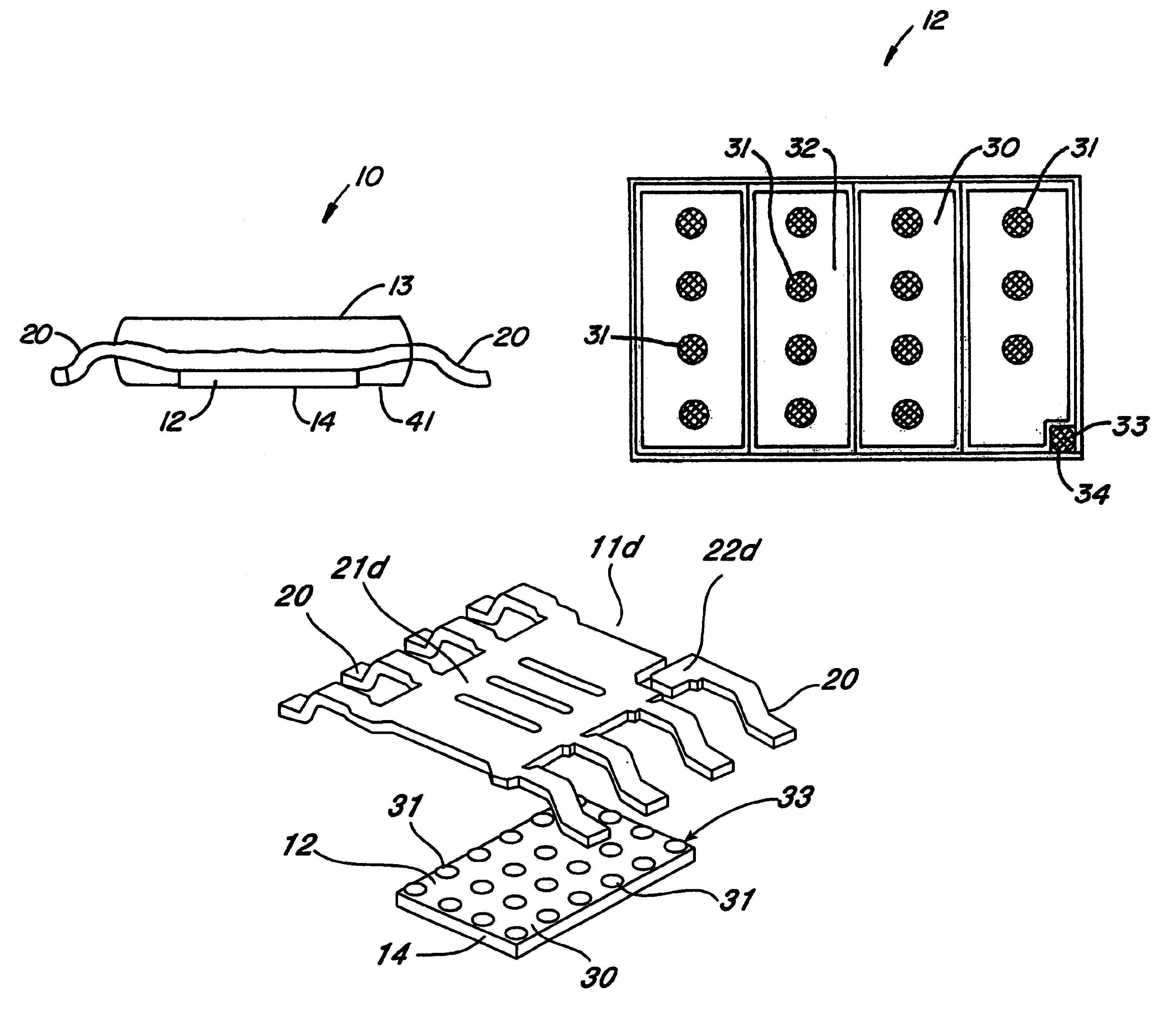
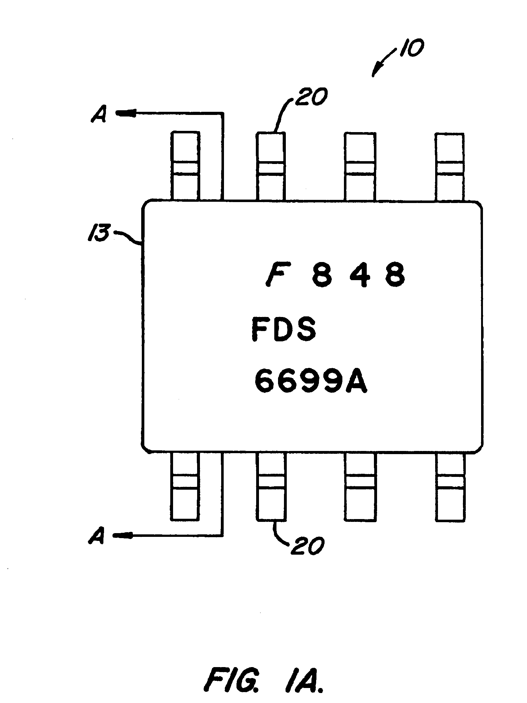
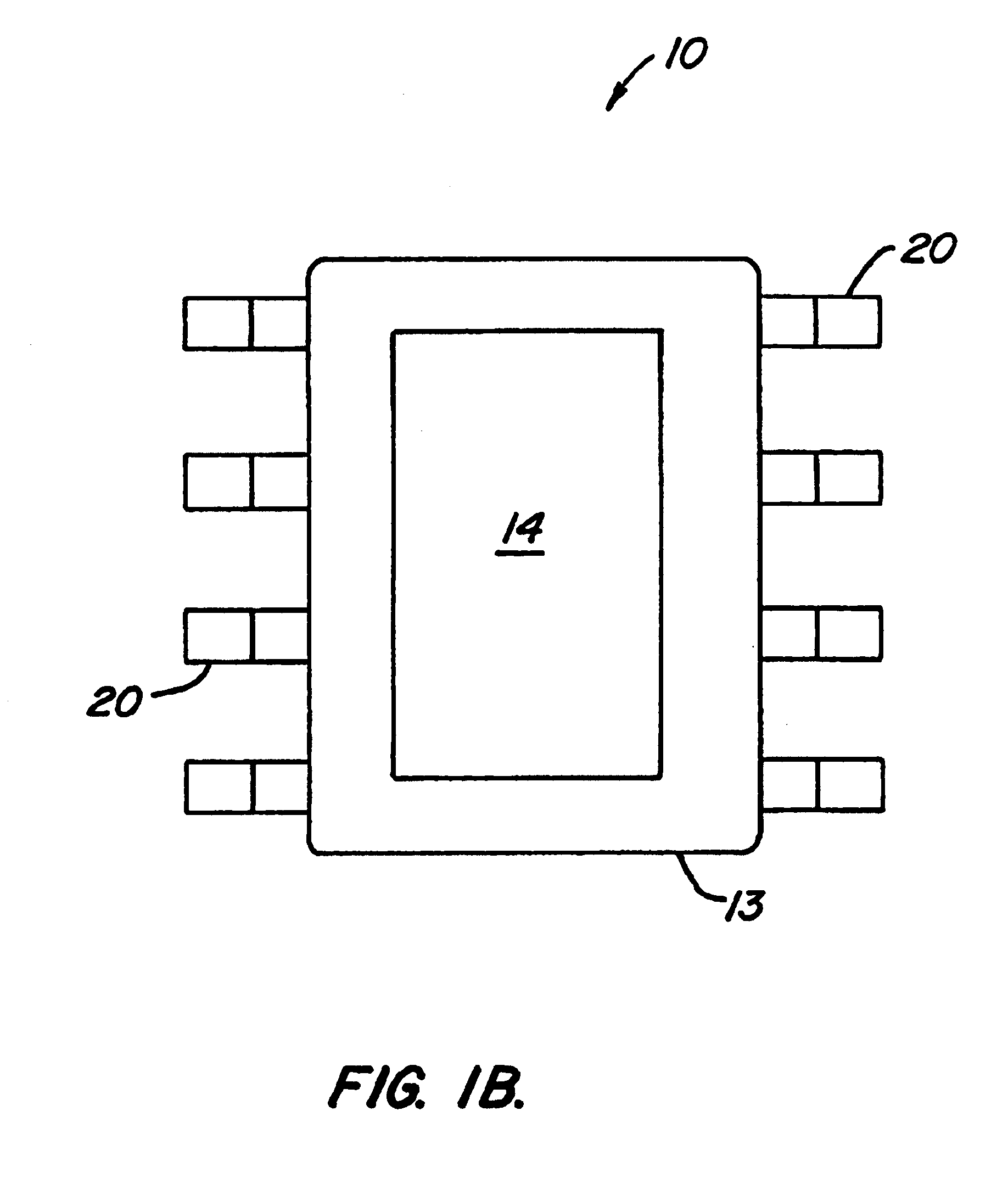
A chip device or semiconductor device 10 includes a leadframe 11, a chip or die 12 and a mold compound or body 13. Preferably, backside 14 of the die is metallized.

FIG. 2 illustrates a leadframe 11a including a plurality of leads 20 and a die attach pad 21a and post 22a. Preferably, the leadframe consists of a copper base and is either silver plated or nickel plated on the die attach pad and post. FIG. 3 illustrates a leadframe 11b similar to leadframe 11a. Leadframe 11b includes two die attach pads and posts 22b and thus is used for a chip device that includes two chips or dies. Thus, chip devices with multiple dies may be made. While FIG. 3 illustrates two die attach pads, it should be readily apparent to those skilled in the art that leadframes with more than two die attach pads may be used, and hence, chip devices with more than two dies may be made.

FIG. 3A illustrates leadframe 11c that includes a common die attach pad 21c for two dies thus providing a die-to-die connection. By...


PUM


Abstract

A chip device that includes a leadframe, a die and a mold compound. The backside of the die is metallized and exposed through a window defined within a mold compound that encapsulates the die when it is coupled to the leadframe. Leads on the leadframe are coupled to source and gate terminals on the die while the metallized backside of the die serves as the drain terminals.

Description

1. Field of the InventionThe present invention relates to an improved package and method of packaging for a flip chip, and more particularly, to a flip chip wherein a die is attached to a leadframe that is then placed within a thinner package such that the back side of the die is exposed.2. Description of the Prior ArtIn power transistor packages, those in the art are generally still using chip and wire bond interconnect technology. It is difficult to simplify the manufacturing process flow as all process steps, such as, for example, die attach, wire bond, and molding are required. As a result, there is a limit placed on the maximum size for the die. Thus, power transistor packages are suited for single die applications since formation of an isolated metal pad for power transistor packages that include multiple dies is very difficult.Recent attempts to improve packaging of chip devices have included directly coupling lead frames to the die. However, this technology does not lend its...

Claims


Application Information

Patent Timeline
Patent Type & Authority Patents(United States)
IPC IPC(8): H01L23/48H01L23/495H01L23/28H01L23/31H01L21/76H01L23/52
CPCH01L23/3121H01L23/3185H01L23/49531H01L23/49562H01L23/544H01L2223/54406H01L2223/54433H01L2223/54486H01L2924/13091H01L2924/0002H01L2924/00
Inventor JOSHI, RAJEEVTANGPUZ, CONSUELO N.MANATAD, ROMEL N.
Owner SEMICON COMPONENTS IND LLC
Why Eureka
Try Eureka