Sensor package and method of manufacturing the same

a technology of sensor and manufacturing method, applied in the field of semiconductor package structure, can solve the problems of high accuracies required for through silicon, electrical fingerprint, and complicated molding technology of sensors, and achieve the effect of reducing manufacturing cost and thinning packages

Active Publication Date: 2019-04-23
PHOENIX PIONEER TECH
View PDF9 Cites 0 Cited by
  • Summary
  • Abstract
  • Description
  • Claims
  • Application Information

AI Technical Summary

Benefits of technology

[0010]It is therefore an object of the present invention to provide a sensor package and a method of manufacturing the sensor package with a panel level packaging process and a through outside silicon via (TOSV) technology, which provides thinner packages and reduces the manufacturing cost.
[0015]Accordingly, the via plugs with truncated cone shapes are formed in the encapsulation layer through TOSV technology in the sensor package of the present invention. The ratio of the first diameter of via plug at the sensor side to the second diameter of via plug at the opposite side is 40%-80%. Since such via plugs are utilized as the electrical connections between the sensor and the external PCB, thinner packages and lower manufacturing cost are achieved in the present invention. In addition, the manufacturing method of the present invention is carried out with a panel level packaging process to handle large numbers of sensors in batch. Thereby, the present invention yields several times as much as the prior art, and the production efficiency is effectively improved.

Problems solved by technology

However, the molding technology for sensors is more complicated than the molding technology for integrated circuits.
This creates an electrical fingerprint.
However, high accuracies are required for the through silicon via process of the via plugs 36, because a tiny mistake in the through silicon via process may cause a fail chip.
Accordingly, the through silicon via process leads to a high manufacturing cost, which is unfavorable to the market.

Method used


Image

  • Sensor package and method of manufacturing the same
  • Sensor package and method of manufacturing the same
  • Sensor package and method of manufacturing the same

Examples


first embodiment

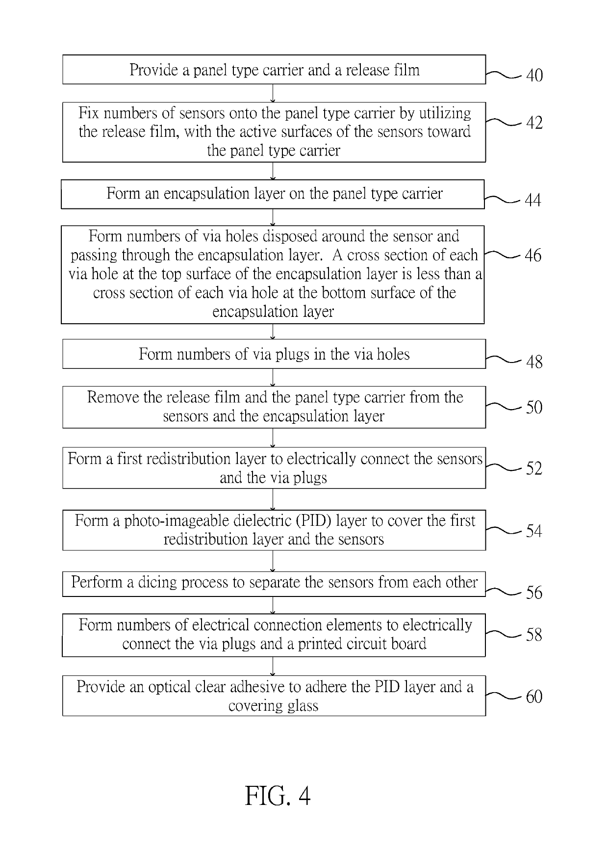
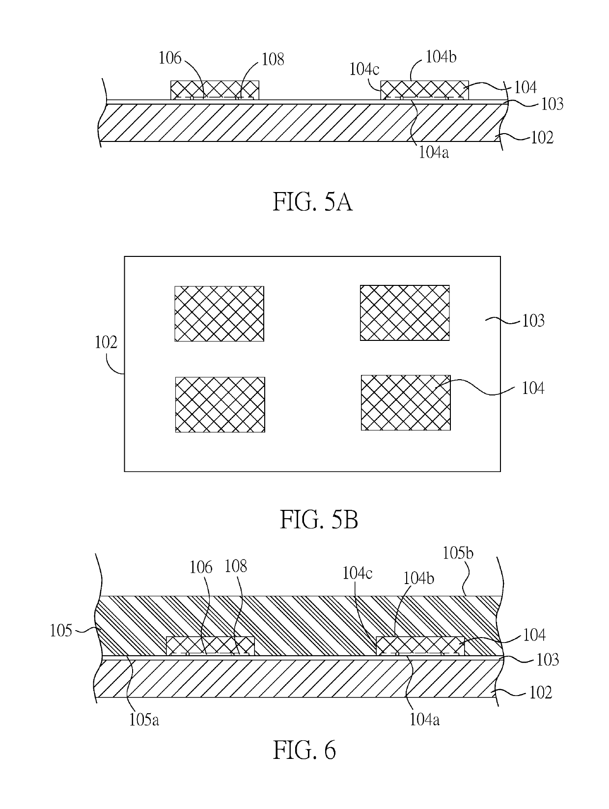
[0026]FIG. 4 is a flow chart showing a method of manufacturing sensor packages 100 according to the present invention. FIG. 5A, FIG. 5B and FIG. 6 through FIG. 12 are schematic diagrams illustrating a method of manufacturing sensor packages 100 according to the present invention, in which FIG. 5B shows a top view of the intermediate sensor package made in FIG. 5A, and FIG. 9B shows a top view of the intermediate sensor package manufacturing method in FIG. 9A.

[0027]As shown in FIG. 5A, FIG. 5B and the step 40 of FIG. 4, a panel type carrier 102 and a peelable film 103 are first provided. The peelable film 103 is disposed on a surface of the panel type carrier 102. The peelable film 103 may be a release film. The panel type carrier 102 may include a metal material, such as iron, steel or cupper.

[0028]As shown in FIG. 5A, FIG. 5B, and the step 42 of FIG. 4, a sensor adhering process is subsequently performed. In the sensor adhering process, numbers of sensors 104 are provided. The sens...

second embodiment

[0045]The second embodiment can be applied to various products. For example, when the sensors 104 are the CMOS image sensors, the structure of the sensor package 200 can increase the sensitivity of the sensors 104. The recesses of the PID layer 140 located on the sensing areas 106 are apertures for the sensor package 200. Since the optical adhesive 142 are transparent for external light, the sensor package 200 can access amounts of light.

[0046]FIG. 14 is a schematic diagram illustrating a method of manufacturing sensor packages 300 according to the third embodiment of the present invention. The difference between the third embodiment and the first embodiment is that the third embodiment further includes a second redistribution layer 134 and a dielectric layer 144.

[0047]As shown in FIG. 14, the second redistribution layer 134 and the dielectric layer 144 are formed on the encapsulation layer 105, after forming the via plugs 120 (after the step 50), and before forming the electrical c...


PUM


Abstract

A sensor package includes a sensor, an encapsulation layer, a redistribution layer, a photo-imageable dielectric (PID) layer and via plugs. The encapsulation layer exposes the active surface of the sensor, and the top surface of the encapsulation layer is coplanar with the active surface of the sensor. The redistribution layer covers the top surface of the encapsulation layer and the active surface of the sensor. The PID layer covers the redistribution layer, the encapsulation layer and the active surface of the sensor. The via plugs are disposed around the sensor and through the encapsulation layer. The via plugs are electrically connected to the redistribution layer and the active surface of the sensor. The cross section of the via plug at the top surface of the encapsulation layer has a first hole diameter, and the cross section of the via plug at the bottom surface of the encapsulation layer has a second hole diameter. The first hole diameter is less than the second hole diameter.

Description

CROSS REFERENCE TO RELATED APPLICATIONS[0001]This Non-provisional application claims priority under 35 U.S.C. § 119(a) on Patent Application No. 106133542 filed in Republic of China on Sep. 29, 2017, the entire contents of which are hereby incorporated by reference.BACKGROUND1. Technical Field[0002]This invention relates to a semiconductor package structure and a manufacturing method thereof, in particular, to a sensor package and a manufacturing method thereof.2. Description of Related Art[0003]A sensor is an electronic component, module, or subsystem to detect events or changes in its environment, and to send the information to other electronics. With advances in various sensing technologies and micro-machinery, sensors are now widely used in everyday objects, such as image sensors and fingerprint sensors applied to portable consumer electronics.[0004]An image sensor or imaging sensor is a sensor that detects and conveys the information that constitutes an image. A fingerprint sen...

Claims


Application Information

Patent Timeline
Patent Type & Authority Patents(United States)
IPC IPC(8): H01L31/0203H01L27/146
CPCH01L27/14618H01L27/14636H01L27/14687H01L2224/18H01L2224/48091H01L2924/181H01L2224/11H01L2224/04105H01L2224/96H01L2924/00014H01L2924/00012
Inventor HSU, CHE-WEIHSU, SHIH-PING
Owner PHOENIX PIONEER TECH
Why Eureka
Try Eureka