Semiconductor device chip scale surface assembling and packaging, and mfg. method therefor

A technology for device packaging and manufacturing methods, applied in the fields of semiconductor/solid-state device manufacturing, semiconductor devices, semiconductor/solid-state device components, etc., can solve the problems of expensive, fragile wire bonding, time-consuming, etc. The effect of on-resistance

Inactive Publication Date: 2004-11-24
VISHAY INTERTECHNOLOGY INC
View PDF0 Cites 0 Cited by
  • Summary
  • Abstract
  • Description
  • Claims
  • Application Information

AI Technical Summary

Problems solved by technology

[0003] Often an expensive, time-consuming process, the resulting semiconductor package is significantly larger than the die itself, using up excess "scarce space" on the PCB
Also, the wire bonds are fragile, introducing a lot of resistance between the die pad and the package's leads

Method used


Image

  • Semiconductor device chip scale surface assembling and packaging, and mfg. method therefor
  • Semiconductor device chip scale surface assembling and packaging, and mfg. method therefor
  • Semiconductor device chip scale surface assembling and packaging, and mfg. method therefor

Examples


Embodiment Construction

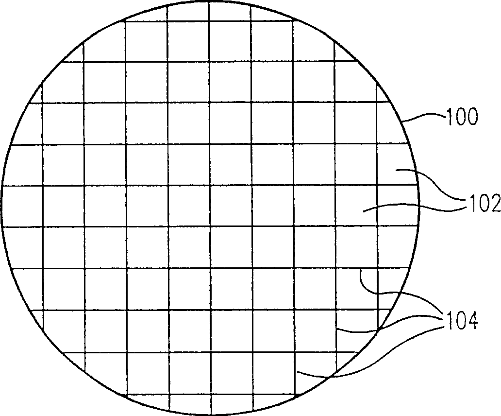
[0032] Processing of the semiconductor wafer forms a rectangular array of dies. exist figure 1 A top view of wafer 100 and die 102 is shown in . The dies are separated by an orthogonal network of scribe lines 104 , typically sawing to separate the dies 102 .

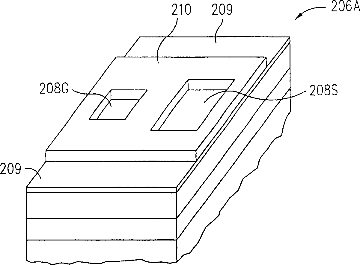
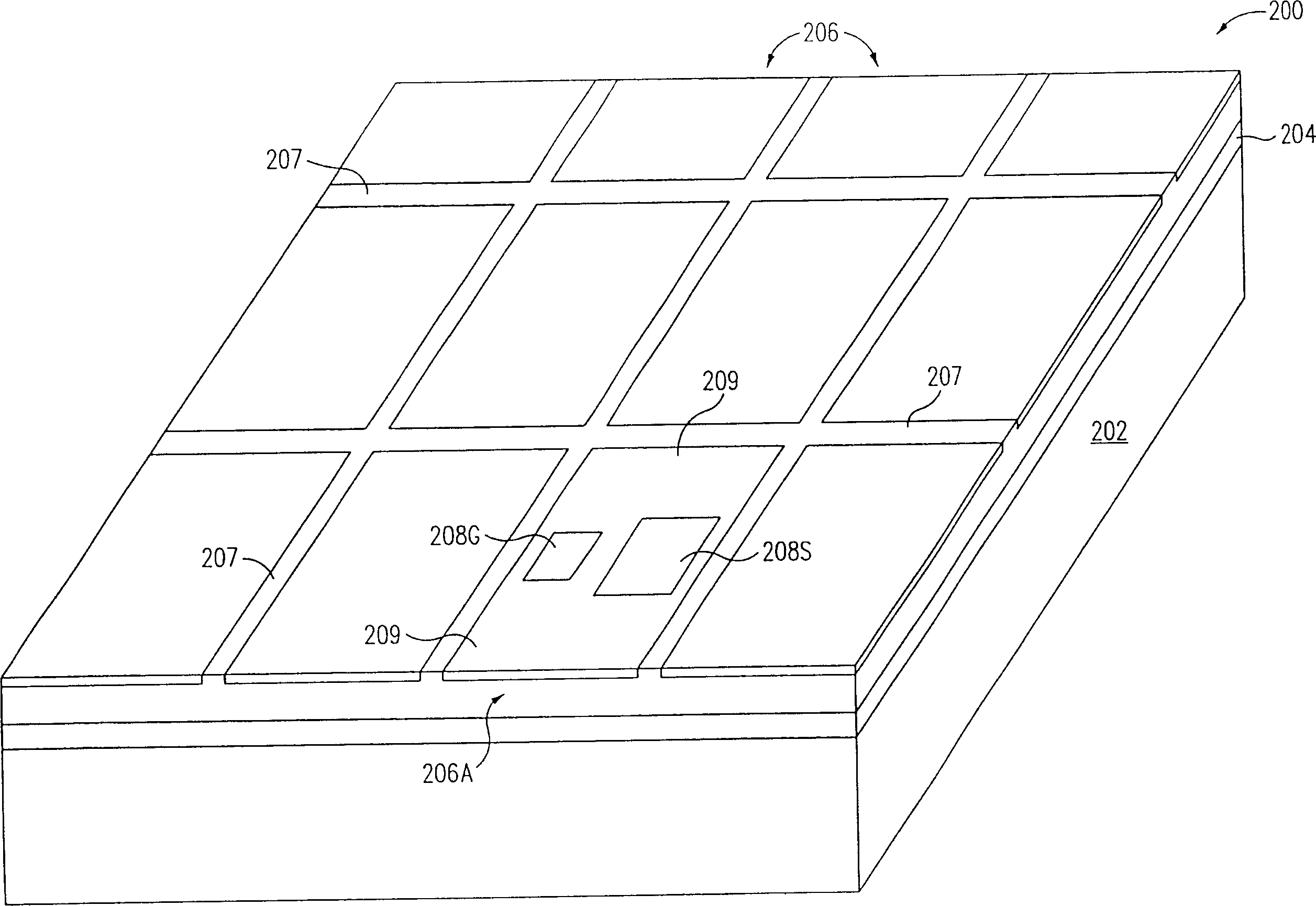
[0033] The invention is described below with reference to the packaging of a vertical power MOSFET, which typically has source and gate terminals on the front side and a drain terminal on its back side. However, it should be understood that the basic principles of the present invention can be used to manufacture packages for any type of semiconductor die with terminals on the front and back, including diodes, bipolar transistors, junction field effect transistors (JFETs), and integrated circuits of various types. (IC). As used herein, "front" of a die refers to the side of the die that contains the electrical components and / or most of the connection pads; "back" refers to the quilt side of the die.

[0034] A semicon...


PUM


Abstract

This semiconductor surface mount package is relatively inexpensive to produce and has a footprint that is essentially the same size as the die. A conductive substrate is attached to the back side of a wafer and is in electrical contact with a terminal on the back side of each die in the wafer. A nonconductive overcoat is formed and patterned on the front side of the wafer, leaving a portion of the passivation layer and the connection pads for the dice exposed, each of the connection pads being coated with a solderable metal layer. The assembly is then sawed in perpendicular directions along the scribe lines between the dice, but the saw cuts do not extend all the way through the substrate, which remains intact at its back side. The parallel cuts in one direction are broken to produce die strips which are mounted, sandwich-like, in a stack, with one side of the strips exposed. A metal layer is sputtered or evaporated on one side of the stack; the stack is turned over and a similar process is performed on the other side of the stack. The resulting metal layers are deposited on front side of the die and extend along the edges of the die to the edges and back side of the substrate. The metal is not deposited on the surfaces of the overcoat. The strips in the stack are then separated, and the saw cuts in the perpendicular direction are broken to separate the individual dice. A thick metal layer is plated on the sputtered or evaporated layers to establish a good electrical connection between the front side and the terminal on the back side of each die. The resulting package thus includes a metal layer which wraps around the edges of the die to form an electrical connection between a location on the front side of the die and the conductive substrate. The package is essentially the same size as the die. In an alternative embodiment, a nonconductive substrate is used and vias are formed in the substrate and filled with metal to make electrical contact with the terminal on the back side of the die.

Description

technical field [0001] The invention relates to a semiconductor device package and a manufacturing method thereof. Background technique [0002] After the processing of the semiconductor wafer is complete, the resulting integrated circuit (IC) chips or die must be separated and packaged in such a way that they can be connected to external circuits. There are many known packaging techniques today. Most involve mounting the die on a lead frame, attaching the die mount to the lead frame by wire bonding or other means, and then encapsulating the die and bond wires in a plastic enclosure while the lead frame is removed from the enclosure. stick out. Sealing is usually done by injection moulding. The leadframe is then trimmed to remove the tie bars that hold it together, and the leads are bent to mount the package on a flat surface, typically a printed circuit board (PCB). [0003] Often an expensive, time-consuming process, the resulting semiconductor package is significantly...

Claims


Application Information

Patent Timeline
Patent Type & Authority Patents(China)
IPC IPC(8): H01L23/12H01L21/301H01L21/60H01L21/98H01L23/498H01L25/065H01L29/78
CPCH01L2225/06517H01L2924/0002H01L2225/06513H01L2225/06586H01L25/50H01L23/49805H01L25/0657H01L2924/12044H01L2225/06551H01L2924/09701H01L2924/00H01L21/60
Inventor 费利克斯·赞德曼Y·默罕穆德·卡塞姆何约瑟
Owner VISHAY INTERTECHNOLOGY INC
Why Eureka
Try Eureka