Ultrathin fingerprint identification system-level packaging piece adopting through silicon via and bare die for molding

A system-level packaging and fingerprint recognition technology, which is applied to electrical components, electric solid-state devices, semiconductor devices, etc., can solve problems such as the distance between the lifting sensing area and the outside of the package, and the lack of integration

Inactive Publication Date: 2016-12-21
HUATIAN TECH XIAN
View PDF4 Cites 0 Cited by
  • Summary
  • Abstract
  • Description
  • Claims
  • Application Information

AI Technical Summary

Problems solved by technology

In many current chip processes, the chip pads are generally located on the same surface. If the chip pads are led out by bonding wires, the height of the bonding wires will inevitably increase the di

Method used


Image

  • Ultrathin fingerprint identification system-level packaging piece adopting through silicon via and bare die for molding
  • Ultrathin fingerprint identification system-level packaging piece adopting through silicon via and bare die for molding
  • Ultrathin fingerprint identification system-level packaging piece adopting through silicon via and bare die for molding

Examples


Embodiment Construction

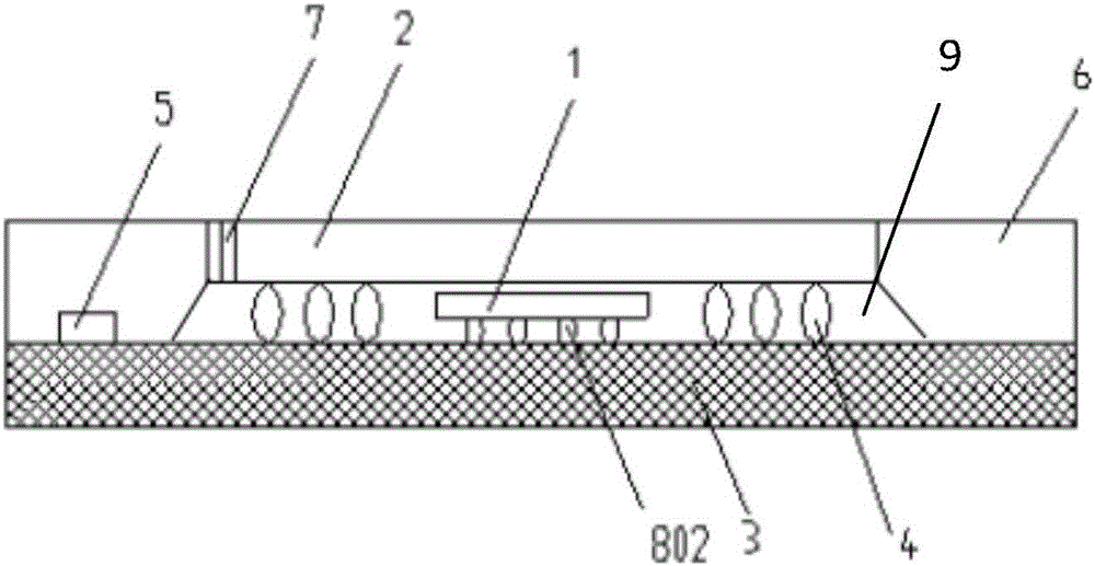
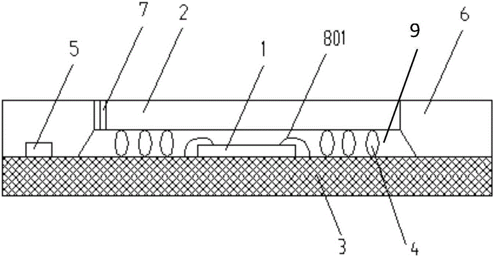
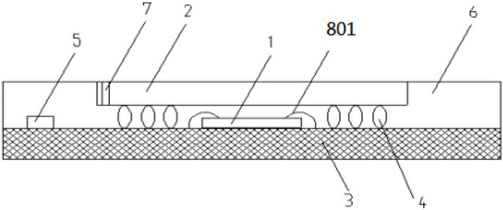
[0015] An ultra-thin fingerprint identification system-level package adopting through-silicon vias and bare core plastic packaging, including a sensor chip 2, solder balls 4, filling glue 9, a substrate 3, and a plastic package 6, and the sensor chip 2 runs through There are through-silicon vias 7 , the sensor chip 2 is connected to the substrate 3 through solder balls 4 , the filler 9 fills the area between the solder balls 4 , and the plastic package 6 wraps the sensor chip 2 , the filler 9 and most of the substrate 3 . The package has components 5 connected to the substrate 3 , which are arranged side by side on the same substrate 3 with the sensor chip 2 and wrapped by a plastic package 6 . The package has a functional chip 1, the functional chip 1 is located in the space between the back of the sensing chip 2 and the substrate 3, and is connected to the substrate 3 through solder balls 802, and the filling glue 9 covers the functional chip 1 and the solder balls 802. The ...


PUM


Abstract

The invention discloses an ultrathin fingerprint identification system-level packaging piece adopting through silicon via and a bare die for molding, which comprises a sensing chip, solder balls, a filling adhesive, a substrate and a molding body, wherein the through silicon via passes through the sensing chip; the sensing chip is connected with the substrate via the solder balls; areas among the solder balls are filled with the filling adhesive; and the molding body coats the majority of the sensing chip, the filling adhesive and the substrate. The ultrathin fingerprint identification system-level packaging piece adopting through silicon via and a bare die for molding has the advantages of an ultrathin structure and high sensitivity.

Description

technical field [0001] The invention relates to the field of integrated circuits, in particular to an ultra-thin fingerprint identification system-level package that adopts through-silicon holes and bare core plastic packaging. Background technique [0002] With the continuous improvement of the intelligence of terminal products, various sensor chips emerge in endlessly. For the sensor chip, its biggest feature is that there is a sensing area on the surface of the chip, which interacts with the external stimulus to be recognized to generate electrical signals that the chip can recognize and process. The distance between this area and external stimuli should be as short as possible so that the generated signal can be detected. In many current chip technologies, the chip pads are generally located on the same surface. If the chip pads are led out by bonding wires, the height of the bonding wires will inevitably increase the distance between the sensing area and the outside of...

Claims


Application Information

Patent Timeline
IPC IPC(8): H01L23/31H01L25/00H01L23/52H01L23/48
CPCH01L2224/16225H01L2224/48091H01L2224/48227H01L2924/00014H01L23/31H01L23/48H01L23/52H01L25/00
Inventor 谢建友王奎陈文钊
Owner HUATIAN TECH XIAN
Why Eureka
Try Eureka