Biosensor circuit and sensor array consisting of a plurality of said biosensor circuits and biosensor array

a biosensor circuit and array technology, applied in the direction of radiation intensity measurement, instruments, x/gamma/cosmic radiation measurement, etc., can solve the problems of insufficient structure dimensions, inability to detect electrical signals of nerve cells, and inability to achieve structural dimensions that can be achieved, etc., to achieve high spatial resolution of the sensor array, high integration density of sensor elements, and high degree of miniaturization

Inactive Publication Date: 2006-03-28
INFINEON TECH AG
View PDF16 Cites 120 Cited by
  • Summary
  • Abstract
  • Description
  • Claims
  • Application Information

AI Technical Summary

Benefits of technology

[0053]The substrate of the sensor arrangement is preferably a silicon substrate in particular a silicon wafer or a silicon chip. In this case, the advantages and mature customary processes of silicon microelectronics can be used to produce the sensor arrangement according to the invention.
[0054]The type of coupling between the sensor element and the liquid to be examined may additionally have a capacitive component.
[0055]Refinements of the sensor array according to the invention, which has circuit arrangements according to the invention, are described below. Refinements of the circuit arrangement also apply to the sensor array having circuit arrangements.
[0056]By virtue of the fact that the invention provides a sensor array having a plurality of circuit arrangements, said circuit arrangements being arranged essentially in matrix form in crossover regions of row and column lines and being connected up to the row and column lines, it is possible to achieve a high integration density of sensor elements and a high degree of miniaturization, as a result of which the spatial resolution of the sensor array is high.
[0057]Preferably, in the sensor array, at least a part of the circuit arrangements have a selection element—coupled to the respectively associated row line and / or column line—for selection of the respective sensor arrangement in order to detect a sensor signal of the sensor element of the selected circuit arrangement and / or in order, in the case of the selected circuit arrangement, at least partly to compensate for the alteration of the value of the physical parameter and / or in order to apply the fifth electrical potential to the sensor element of the selected circuit arrangement.
[0058]Such a circuit enables the selection of a sensor element or of a circuit arrangement of the sensor array and is set up in such a way as to provide signals for driving selection elements for example at an end section of row and column lines.

Problems solved by technology

For experimental or apparatus-related reasons, therefore, traditional techniques for deriving neural activity encounter their limits.
By way of example, it is no longer possible to detect electrical signals of a nerve cell by penetrating into individual cells using glass microelectrodes in the case of large cell assemblages having ten thousand or even millions of neurons, even in in-vitro experiments.
However, the use of glass as a substrate for a sensor array has the disadvantage that the structure dimensions that can be achieved are not small enough, and that a sufficiently high spatial resolution of the activity of nerve cells cannot therefore be achieved.
This means, in particular, that static differences in the output signals of the sensor elements (offset), which may be based for example on process fluctuations during the manufacture of the sensor elements, are not permitted to occur.
A direct ohmic contact, that is to say a direct penetration of the particles at an electrically conductive region of the FET, is not possible.
However, this concept has the disadvantage that in each case only one sensor array can be selected at one point in time.
Furthermore, optical MEAs have the disadvantage that they have expensive and complicated components.
Moreover, on account of the use of macroscopic components, such as a laser arrangement, for example, the construction of such sensor arrangements is often high, which counteracts a miniaturization that is striven for.
Since optical MEAs in accordance with the prior art are predominantly formed on the basis of a glass substrate, for example the use of active switching or amplifier units, for example of preamplifiers directly below the electrode, is technologically not possible.
Moreover, in the case of the glass substrate technology, a sufficiently small dimensioning of the sensor elements and a sufficiently small distance between the sensor elements are not possible, so that both the temporal and the spatial resolution of the sensor elements require improvement.
As a result, the maximum number of sensor arrays 104 that can be achieved is greatly restricted.
Furthermore, evaluation of the signals provided at the contact areas 106 requires complicated external evaluation electronics (not shown in FIG. 1), which increase the space requirement of the electrically adjustable multi-electrode array 100.
Furthermore, a significant disadvantage of the electrically addressable MEAs 100 known from the prior art can be seen in the fact that the requirement that the output signals of two different sensors of an MEA 100, given identical input signals, are likewise identical is often not fulfilled.

Method used


Image

  • Biosensor circuit and sensor array consisting of a plurality of said biosensor circuits and biosensor array
  • Biosensor circuit and sensor array consisting of a plurality of said biosensor circuits and biosensor array
  • Biosensor circuit and sensor array consisting of a plurality of said biosensor circuits and biosensor array

Examples


Embodiment Construction

[0068]It should be noted that, in the exemplary embodiments of the sensor array according to the invention that are described below with reference to FIG. 2 to FIG. 19 many of the components described occur in different exemplary embodiments. Such components are in each case provided with the same reference numerals in different exemplary embodiments. Furthermore, the functionality of subcircuits of the different exemplary embodiments of the sensor array according to the invention is also identical in some instances, so that this functionality is not described in detail for every exemplary embodiment and, therefore, reference is made back to other exemplary embodiments.

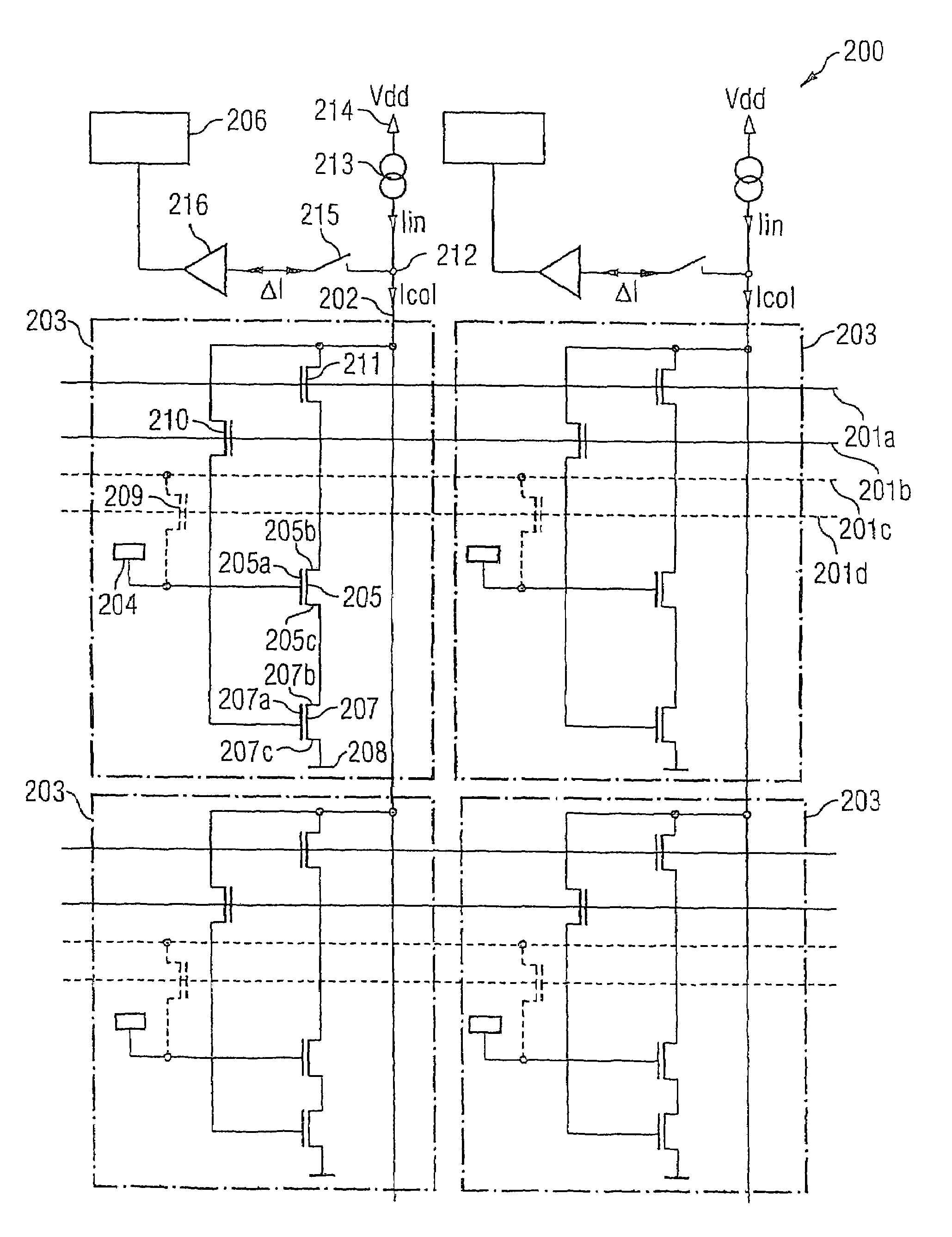
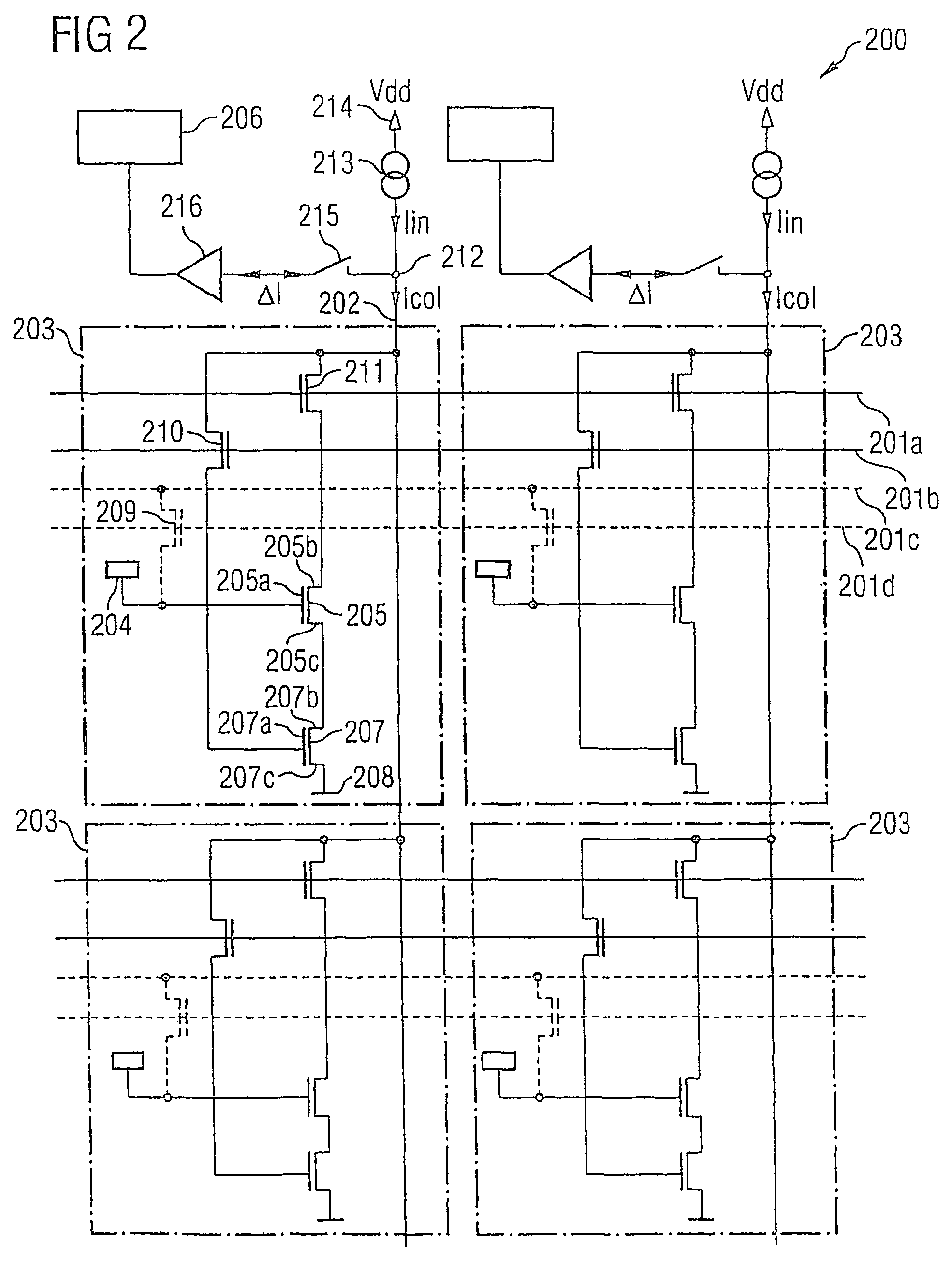
[0069]FIG. 2 shows a sensor array 200 in accordance with a first preferred exemplary embodiment of the invention.

[0070]The sensor array 200 has a plurality of biosensor circuit arrangements 203 which are arranged in matrix form in crossover regions of row lines 201a, 201b, 201c, 201d and column lines 202 and are conne...


PUM

PropertyMeasurementUnit
distanceaaaaaaaaaa
threshold voltageaaaaaaaaaa
physical parameteraaaaaaaaaa

Abstract

Biosensor circuit arrangement including a substrate, a sensor element formed in or on a surface region of the substrate with a physical parameter, which is coupled to a substance to be examined, the type of coupling having a resistive component, the sensor element having an electrically conductive sensor electrode that is coupled to the substance to be examined, the sensor element having a measuring transistor the gate terminal of which is coupled to the electrically conductive sensor electrode, and the physical parameter being the threshold voltage of the measuring transistor, and a calibration device formed in or on the substrate, the calibration device being set up such that it is used to at least partly compensate for an alteration of the value of the physical parameter of the sensor element.

Description

CROSS-REFERENCE TO RELATED APPLICATION[0001]This application is a continuation of International Patent Application Serial No. PCT / DE02 / 03613, filed Sep. 25, 2002, which published in German on May 8, 2003 as WO 03 / 038420.FIELD OF THE INVENTION[0002]The invention relates to a circuit arrangement, a sensor array and a biosensor array.BACKGROUND OF THE INVENTION[0003]The network structure of higher animals' brains is of high complexity and is the subject of current research in neurobiology. One aspect of this complexity can be seen in the fact that outwardly discernible functionalities such as memory or object formation is only realized by the interlinking of individual nerve cells. The consequence of this for neurobiological analysis is that the activity of a very large number of nerve cells has to be taken into consideration for understanding the brain. For experimental or apparatus-related reasons, therefore, traditional techniques for deriving neural activity encounter their limits....

Claims


Application Information

Patent Timeline
Patent Type & Authority Patents(United States)
IPC IPC(8): G01N27/416G01N27/414G01N33/487H03F3/45
CPCG01N27/4145H03F3/45188G01N33/4836H03F2203/45352
Inventor EVERSMANN, BJORN-OLIVERJENKNER, MARTINPAULUS, CHRISTIANTHEWES, ROLAND
Owner INFINEON TECH AG
Why Eureka
Try Eureka