Leadframe, semiconductor package and method for producing the same

A lead frame and semiconductor technology, applied in the direction of semiconductor devices, semiconductor/solid-state device components, electric solid-state devices, etc., can solve the problems of limitation improvement, minimum length of bonding wire and height limitation of bonding wire, etc., and achieve the effect of reducing distance

Inactive Publication Date: 2009-12-30
INFINEON TECH AG
View PDF4 Cites 0 Cited by
  • Summary
  • Abstract
  • Description
  • Claims
  • Application Information

AI Technical Summary

Problems solved by technology

However, the nature of the wire bonding process places constraints on the minimum length of the bond wire and the height of the loop of the bond wire
Therefore, the possible improvement of this scheme is limited

Method used


Image

  • Leadframe, semiconductor package and method for producing the same
  • Leadframe, semiconductor package and method for producing the same
  • Leadframe, semiconductor package and method for producing the same

Examples


Embodiment Construction

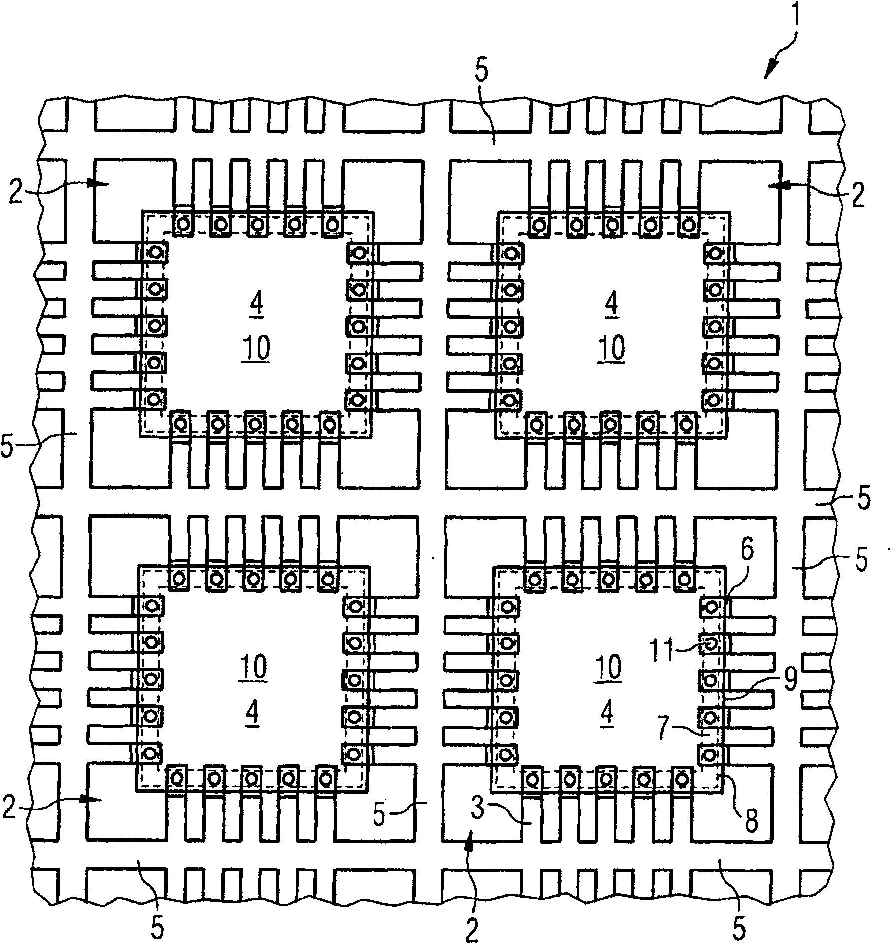
[0086] figure 1 A top view of a portion of a leadframe strip 1 comprising a plurality of packaging locations 2 is shown. exist figure 1 Four packaging locations 2 are shown within the portion shown. Each packaging site 2 is substantially identical and substantially square in the transverse direction. The packaging sites 2 are arranged in rows and columns within the lead frame strip 1 and have a grid configuration.

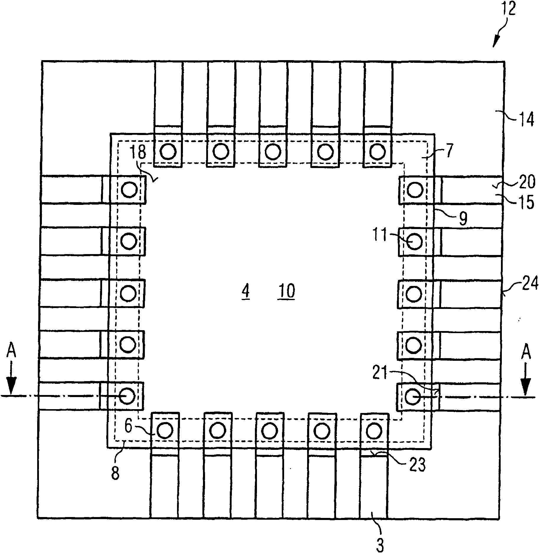
[0087] Each packaging site 2 comprises a plurality of lead fingers 3 laterally surrounding a chip site 4 . Chip site 4 is approximately in the lateral center of package site 2 . Each packaging location 2 is physically connected to its neighbors by tie rods 5 having a grid configuration.

[0088] Lead fingers 3 protrude inwards from tie bars 5 towards the center of each packaging location 2 . exist figure 1 In the example shown, each of the four sides of each packaging location 2 includes five lead fingers 3 located approximately in the lateral center of each...


PUM


Abstract

A semiconductor package includes a lead frame (2) comprising a chip position (4) and a plurality of lead fingers (3). Each lead finger (3) includes a incision (19) in an inner edge providing a chip recess (25). The semiconductor package (12) further includes a semiconductor chip (10) locating in the chip recess (25). The semiconductor chip (10) is arranged with an active surface (17) with a plurality of chip contact pads (16) on each of which an electrically conductive bump (11) is disposed. The inner portions (13) of the lead fingers (3) protrude into the chip position (4) and are electrically connected to the chip contact pads (16) by electrically conductive bumps (11).

Description

technical field [0001] The invention relates to a semiconductor package, the provision of a lead frame and a semiconductor package comprising said lead frame. The present invention also relates to leadless semiconductor packages and methods for manufacturing lead frames and semiconductor packages. Background technique [0002] Existing leadframe based leaded and leadless packages are known to suffer from various technical problems. Differences in the coefficients of thermal expansion between the various components of a typical semiconductor package, such as the semiconductor chip, lead frame, and molding compound, result in deflection and internal stresses within the semiconductor package. It can lead to the formation of cracks and debonding at the interface between the different materials. This in turn may lead to package failure. [0003] The problem of CTE differences is exacerbated by the presence of numerous interfaces within the package itself. For example, interfa...

Claims


Application Information

Patent Timeline
Patent Type & Authority Patents(China)
IPC IPC(8): H01L23/495H01L23/31
CPCH01L24/97H01L2924/01033H01L2924/01005H01L2924/01006H01L2924/01029H01L23/3107H01L2924/01082H01L2924/01079H01L2924/01075H01L2224/16245H01L2224/97H01L23/49548H01L2924/01013H01L2924/181H01L2924/14H01L2224/0557H01L2224/05573H01L2224/056H01L2224/05571H01L2924/00014H01L2224/0554H01L2224/81H01L2924/00H01L2224/05599H01L2224/0555H01L2224/0556
Inventor R·M·西纳加N·坎苏拉特蒂M·雅兹德
Owner INFINEON TECH AG
Why Eureka
Try Eureka