Method of forming a semi-insulating region

a technology of semi-insulating regions and semiconductors, applied in the direction of semiconductor/solid-state device manufacturing, semiconductor devices, electrical equipment, etc., can solve the problems of affecting the method takes too much time, and the chip material and the manufacturing process both affect the size and cost of chips directly, so as to reduce the antenna effect, improve the total coupling effect, and reduce the loss of a chip substra

Inactive Publication Date: 2006-08-17
UNITED MICROELECTRONICS CORP
View PDF6 Cites 1 Cited by
  • Summary
  • Abstract
  • Description
  • Claims
  • Application Information

AI Technical Summary

Benefits of technology

[0018] It is an advantage of the claimed invention that the method of forming a communication chip by utilizing the semi-insulating regions utilizes at least one semiconductor wafer, metal plate, or other substance as the first mask and a photoresist layer as the second mask to perform the high energy particle beam implantation process. Not only are the material compositions of the masks variable, the shapes and the thicknesses of a first pattern and a second pattern, optionally defined in the first mask and in the second mask respectively, can be changed according to the requirements of a specific product. In addition, the implantation energy of the high energy beam of particles can be adjusted. The first mask and the second mask can be simultaneously utilized or only one of them may be utilized. The implantation process may be performed several times as the above-mentioned parameters are adjusted. Utilizing the masks in the present invention method as energy reduction layers, the high energy particles can be implanted into the semiconductor substrate to a predetermined depth accurately so as to form uniform and continuous semi-insulating regions and even to form three dimensional semi-insulating regions in the semiconductor substrate. When applying the present invention method in a practical production line, the effect incurred from the induced current is weakened due to the induced current being confined within each non-insulating region so as to reduce an antenna effect. The substrate loss for a chip is reduced, the total coupling effect is improved, and the noise in a transmission line is decreased. A communication chip with good RF performance is therefore produced.

Problems solved by technology

While integrating all those components, not only the chip volume needs to be shrunk, but also the cost of the discrete devices could not be raised.
In addition, the chip materials and the manufacturing process both impact the size and the cost of chip directly.
However, this method takes too much time (10 to 100 days).
However, the prior art methods are not suitable for mass production at all since the photoresist layer utilized in the clean room, even the thick film photoresist having a thickness of approximate 200 to 300 μm, is unable to completely block the beam of particles with such a high energy.
This kind of mask, although suitable for certain environments, is not suitable to be used in the clean room due to contamination issues.
However, to implant the communication chip with a beam of high energy particles to reduce the loss of silicon substrate, or the loss of another substrate is an inevitable process step.

Method used


Image

  • Method of forming a semi-insulating region
  • Method of forming a semi-insulating region
  • Method of forming a semi-insulating region

Examples


Embodiment Construction

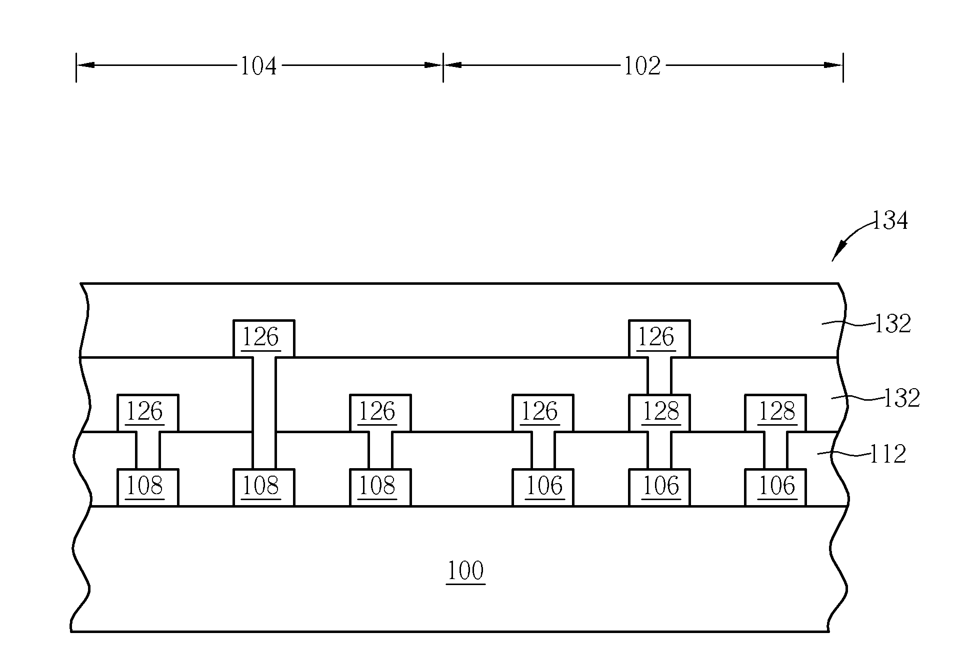
[0032] Please refer to FIG. 5 to FIG. 9 that are schematic diagrams of fabricating a communication chip by utilizing a semi-insulating region 104 according to the first preferred embodiment of the present invention. As shown in FIG. 5, the communication chip according to the first preferred embodiment of the present invention is fabricated on a semiconductor wafer 100. A non-insulating region 102 and a semi-insulating region 104 are comprised on a surface of the semiconductor substrate 100. The non-insulating region 102 is usually used for forming active devices, and the semi-insulating region 104 is usually used for forming passive devices. The semiconductor substrate 100 of the present invention is a silicon substrate, a germanium substrate, a gallium arsenide substrate, a silicon germanium substrate, an indium phosphide substrate, a gallium nitride substrate, a silicon carbide substrate, or a silicon on insulator (SOI) substrate.

[0033] According to the first preferred embodiment...


PUM


Abstract

A semiconductor substrate is provided, and at least one first mask is formed above the semiconductor substrate. The first mask has a plurality of thicknesses and blocks at least one semi-insulating region. A second mask is thereafter formed on a surface of the semiconductor substrate. The second mask covers the semi-insulating region. The semi-insulating region is implanted with a high energy beam of particles by utilizing the second mask and the first mask as particle hindering masks. Finally, the second mask is removed.

Description

CROSS REFERENCE TO RELATED APPLICATIONS [0001] This is a continuation-in-part of U.S. application Ser. No. 10 / 907,777, filed Apr. 15, 2005, which itself is a division of U.S. application Ser. No. 10 / 605,681 filed Oct. 17, 2003.BACKGROUND OF THE INVENTION [0002] 1. Field of the Invention [0003] The present invention relates to a method of forming a semi-insulating region, and more particularly, to a method of forming a semi-insulating region applied to a radio frequency chip (RF chip) and integrated with very large scale integrated circuit (VLSI circuit) process. [0004] 2. Description of the Prior Art [0005] The global wireless communication market is developing rapidly; the wireless communication business is thus becoming a rising star. Though the wireless communication products are different from each other due to the combinations of system configurations, user's applications, modulation methods, and channel receiving methods, the key components of them are typically comprised in t...

Claims


Application Information

Patent Timeline
Patent Type & Authority Applications(United States)
IPC IPC(8): H01L31/0328
CPCH01L21/263H01L21/82H01L27/06H01L27/08
Inventor LAI, JOEYLUR, WATER
Owner UNITED MICROELECTRONICS CORP
Why Eureka
Try Eureka