BSI process deep trench isolation manufacturing method

A technology of deep trench isolation and manufacturing method, which is applied in radiation control devices, electrical components, diodes, etc., and can solve problems such as increased random telegraph noise, large plasma damage, increased dark current, and white-spot pixels.

Pending Publication Date: 2020-12-04
SHANGHAI HUALI INTEGRATED CIRCUTE MFG CO LTD
View PDF4 Cites 1 Cited by
  • Summary
  • Abstract
  • Description
  • Claims
  • Application Information

AI Technical Summary

Problems solved by technology

[0004] 1. Cause a lot of plasma damage, increase dark current and defects such as white dot pixels, and the RTS performance is also very poor
[0005] 2. The key size of deep trench isolation metal filling is large, which causes antenna effect and increases random telegraph noise

Method used


Image

  • BSI process deep trench isolation manufacturing method

Examples


no. 1 example

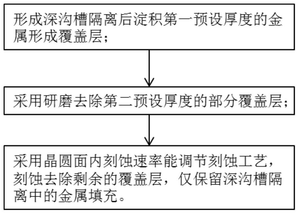
[0026] The first embodiment, such as figure 1 As shown, the present invention provides a BSI process deep trench isolation manufacturing method, which can be applied in the BSI process of 55nm, comprising the following steps:

[0027] S1, after forming the deep trench isolation by etching, deposit a metal with a first predetermined thickness by PVD process, fill the deep trench isolation and form a covering layer on the surface and both sides of the deep trench isolation;

[0028] S2, using grinding to remove part of the covering layer with a second preset thickness;

[0029] S3, etching to remove the remaining cover layer, leaving only the metal filling in the deep trench isolation;

[0030] Wherein, when implementing step S3, the etching rate in the wafer plane can be adjusted.

no. 2 example

[0031] In the second embodiment, the present invention provides a BSI process deep trench isolation manufacturing method, which can be applied to a 55nm BSI process, including the following steps:

[0032] S1, after forming the deep trench isolation by etching, deposit metal tungsten with a first predetermined thickness by PVD process, fill the deep trench isolation and form a covering layer on the surface and both sides of the deep trench isolation;

[0033] S2, using chemical mechanical grinding to remove part of the covering layer with a second preset thickness;

[0034] S3, the remaining cover layer is removed by plasma etching, and only the metal filling in the deep trench isolation is reserved.

no. 3 example

[0035] In the third embodiment, the present invention provides a BSI process deep trench isolation manufacturing method, which can be applied to a 55nm BSI process, including the following steps:

[0036] S1, after etching to form deep trench isolation, deposit metal tungsten with a thickness of 2000-4000 angstroms by PVD process, fill the deep trench isolation and form a covering layer on the surface and both sides of the deep trench isolation;

[0037] S2, using chemical mechanical grinding to remove part of the covering layer with a thickness of 500 angstroms-2500 angstroms;

[0038] S3, using plasma etching to remove the remaining cover layer, leaving only the metal filling in the deep trench isolation.

[0039] To further improve the third embodiment above, in step S1, the preferred thickness of metal tungsten deposited by PVD process after etching to form deep trench isolation is 2000 angstroms, 2100 angstroms, 2200 angstroms, 2300 angstroms, 2400 angstroms, 2500 angstro...


PUM

PropertyMeasurementUnit
thicknessaaaaaaaaaa
thicknessaaaaaaaaaa

Abstract

The invention discloses a BSI process deep trench isolation manufacturing method. The method comprises the following steps: conducting etching to form deep trench isolation, then depositing metal witha first preset thickness, fully filling the deep trench isolation, and forming covering layers on the surface and two sides of the deep trench isolation; removing a part of the covering layers with asecond preset thickness by grinding; and conducting etching to remove the residual covering layers by adopting an etching process with an adjustable wafer in-plane etching rate, and only reserving metal filling in the deep trench isolation. According to the invention, the in-plane uniformity of the wafer can be improved, and the problem of insufficient wafer edge windows is solved; and the metalon the surface of the deep trench isolation is removed in two steps, and the size of the metal on the top of the deep trench isolation can be adjusted, so antenna effect is reduced, and RTS is reduced.

Description

technical field [0001] The invention relates to the field of integrated circuit manufacturing, in particular to a deep trench isolation manufacturing method for BSI technology. Background technique [0002] BSI (backside illuminated CIS): After thinning the silicon wafer, CF and Micro Lens are built on the back of the photodiode. The light enters from the back, which increases the photosensitive area of ​​the photoelectric element and reduces the loss of light when it passes through wiring, which can greatly improve CIS light-sensing ability in low-light environment; BSI technology has raised the sensitivity of CMOS imaging to a new level. The lenses are arranged on the silicon substrate behind the sensor, rather than in front, where the wiring limits light absorption. Compared with the old technology, the sensitivity and light absorption of this technology are increased by 40%, and it can also form finer pixels. [0003] Random telegraph noise (RTS): It is an important pa...

Claims


Application Information

Patent Timeline
Patent Type & Authority Applications(China)
IPC IPC(8): H01L27/146
CPCH01L27/14687H01L27/14689H01L27/1463H01L27/14632H01L27/1464H01L27/14643
Inventor 赵春山康柏张武志曹亚民周维
Owner SHANGHAI HUALI INTEGRATED CIRCUTE MFG CO LTD
Why Eureka
Try Eureka