A semiconductor resistance bridge packaging structure and process

A technology of packaging structure and resistance bridge, applied in the direction of semiconductor devices, semiconductor/solid-state device manufacturing, semiconductor/solid-state device components, etc., can solve the problems of poor dimensional consistency, low packaging efficiency, high packaging cost, and achieve resistance to external shocks. Strong, simple packaging structure, high packaging efficiency

Active Publication Date: 2020-04-10
JACAL ELECTRONICS WUXI
View PDF7 Cites 0 Cited by
  • Summary
  • Abstract
  • Description
  • Claims
  • Application Information

AI Technical Summary

Problems solved by technology

[0002] Existing resistor bridge packages usually install semiconductor resistor chips in the cavities of metal or ceramic bases (such as TO-shaped metal shells, pin pins, or surface-mounted ceramic bases, etc.), and use metal wires (such as gold wires / Gold strip or aluminum wire / aluminum strip, etc.) to interconnect the lead-out pad of the chip with the outer pin of the base, and then wrap the interconnection wire with insulating glue (including the chip bonding pad), the resistance of the semiconductor resistor chip The bridge area is exposed, or chip bonding, wire bonding, and encapsulation are performed on the printed circuit board (PCB). These all have many steps in the packaging process and large package size. The packaging is carried out one by one, and the packaging efficiency is low. , high packaging cost, and poor dimensional consistency after packaging, it cannot meet the requirements of automatic placement process

Method used


Image

  • A semiconductor resistance bridge packaging structure and process
  • A semiconductor resistance bridge packaging structure and process
  • A semiconductor resistance bridge packaging structure and process

Examples


Embodiment

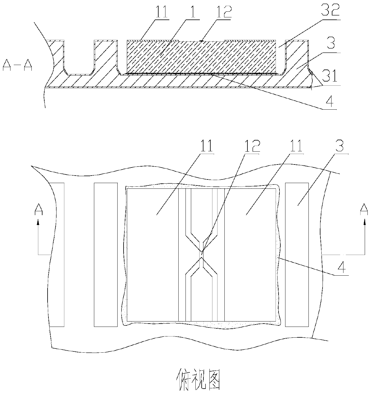
[0031] Embodiment: a kind of size is 2.00mm * 1.20mm * 0.50mm (1206 type) surface mounting semiconductor resistance bridge packaging structure and packaging process, comprising the following steps:

[0032] First, thin the semiconductor resistance bridge wafer to 340 μm; paste a 20 μm thermosetting high-temperature epoxy resin DAF film on the semiconductor resistance bridge wafer with a DAF film laminating machine as the insulating adhesive layer 4; use the semiconductor resistance bridge wafer as Cut and separate the 1.20mm×1.10mm×0.30mm semiconductor resistance bridge chip 1 by emery wheel dicing machine; use the online thermosetting chip loading machine to put the semiconductor resistance bridge chip 1 into the 0.45mm thick C194 copper plate and etch the cavity depth 0.35mm mm, with a size of 1.50mm×1.20mm on the electrode 4, the resistance bridge chip 1 and the electrode 3 are firmly bonded, such as figure 1 ;

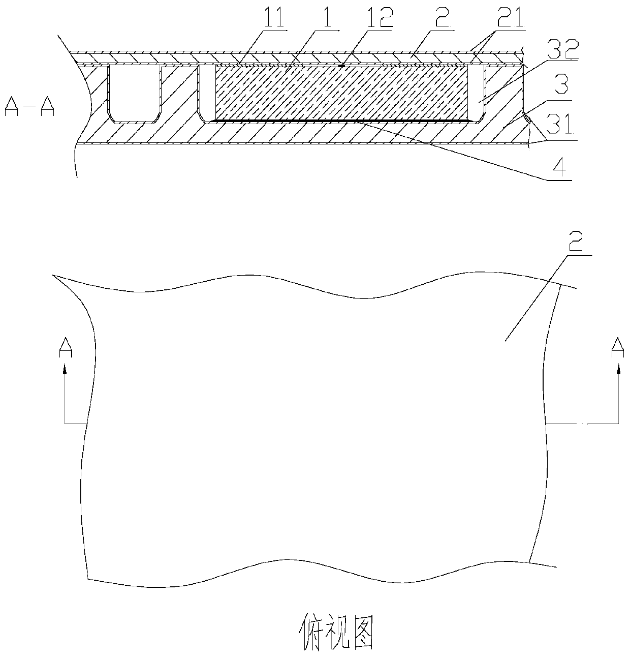
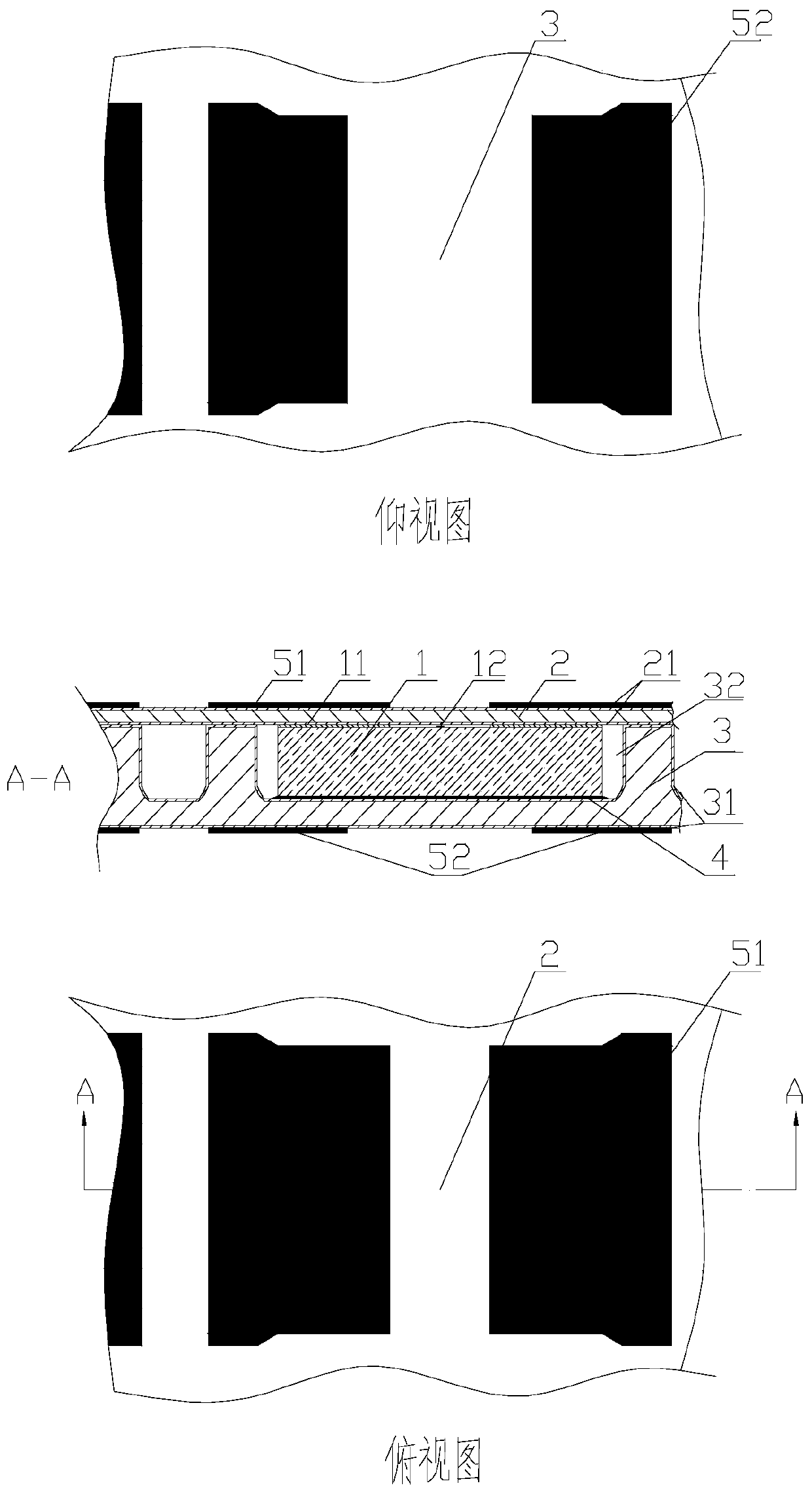
[0033] Secondly, use a C194 copper foil with a thickness of ...


PUM

PropertyMeasurementUnit
thicknessaaaaaaaaaa
thicknessaaaaaaaaaa

Abstract

The invention discloses a semiconductor resistance bridge packaging structure and process. The packaging structure is a two-layer structure, and comprises a semiconductor resistance bridge chip, two welding pieces, two electrodes and a layer of reinforcing insulation glue. The two leading-out terminal soldering pads of the semiconductor resistance bridge chip are subjected to sputtering, evaporation and other processes to form solder layers; the copper or copper alloy plate with a certain thickness is etched out of the core cavity through a wet-process semi-etching process, and the solder layers are plated thereon, the semiconductor resistance bridge chip is bonded in the core cavity of the semiconductor resistance bridge chip through the insulating glue, the large board soldering pieces with the solder layers and the two leading-out terminal soldering pads of the resistance bridge chip are welded to the electrodes through heating and pressurizing; a photoresist coats on the surface after the welding and an etching region is exposed and developed; etching is carried out in the wet etching liquid, so that the large board soldering pieces and the semi-etching large boards are disconnected to form two soldering pieces and two electrodes of the semiconductor resistance bridge; finally, the photoresist film, is removed and the product is obtained by inspection and testing. The packaging structure is of a two-layer structure, the packaging structure is simple, the interconnection resistance of the packaging structure is lower, and the external impact resistance is stronger; andthe metal wire bonding, encapsulation and cutting and packaging processes in the semiconductor resistance bridge packaging are replaced by a wet etching process and a heating and pressurizing weldingprocess, so that the packaging efficiency is higher.

Description

technical field [0001] The invention relates to the technical field of electronic packaging, in particular to a semiconductor resistance bridge packaging structure and a packaging process thereof. Background technique [0002] Existing resistor bridge packages usually install semiconductor resistor chips in the cavities of metal or ceramic bases (such as TO-shaped metal shells, pin pins, or surface-mounted ceramic bases, etc.), and use metal wires (such as gold wires / Gold strip or aluminum wire / aluminum strip, etc.) to interconnect the lead-out pad of the chip with the outer pin of the base, and then wrap the interconnection wire with insulating glue (including the chip bonding pad), the resistance of the semiconductor resistor chip The bridge area is exposed, or chip bonding, wire bonding, and encapsulation are performed on the printed circuit board (PCB). These all have many steps in the packaging process and large package size. The packaging is carried out one by one, an...

Claims


Application Information

Patent Timeline
Patent Type & Authority Patents(China)
IPC IPC(8): H01L23/488H01L23/49H01L21/603
CPCH01L23/488H01L23/49H01L24/84H01L2224/84203
Inventor 丁隽马国荣李保云
Owner JACAL ELECTRONICS WUXI
Why Eureka
Try Eureka