LED packaging structure and manufacturing method

A technology for LED packaging and manufacturing methods, applied in electrical components, circuits, semiconductor devices, etc., can solve the problems affecting the reliability of the electrical connection between the chip and the substrate, poor contact, manufacturing bottlenecks, etc., to achieve convenient operation, improve precision, and reduce manufacturing. cost effect

Active Publication Date: 2016-03-09
HONGLI ZHIHUI GRP CO LTD
View PDF3 Cites 11 Cited by
  • Summary
  • Abstract
  • Description
  • Claims
  • Application Information

AI Technical Summary

Problems solved by technology

In this way, during the heating process, the fluorescent adhesive layer will expand due to heat, which will cause unevenness between the fluorescent adhesive layer and the bottom of the chip, which will lead to poor contact, voids or even non-contact phenomena when the chip and the pad on the substrate are bonded, affecting the connection between the chip and the substrate. Reliability of substrate electrical connection
[000

Method used


Image

  • LED packaging structure and manufacturing method
  • LED packaging structure and manufacturing method
  • LED packaging structure and manufacturing method

Examples


Embodiment 1

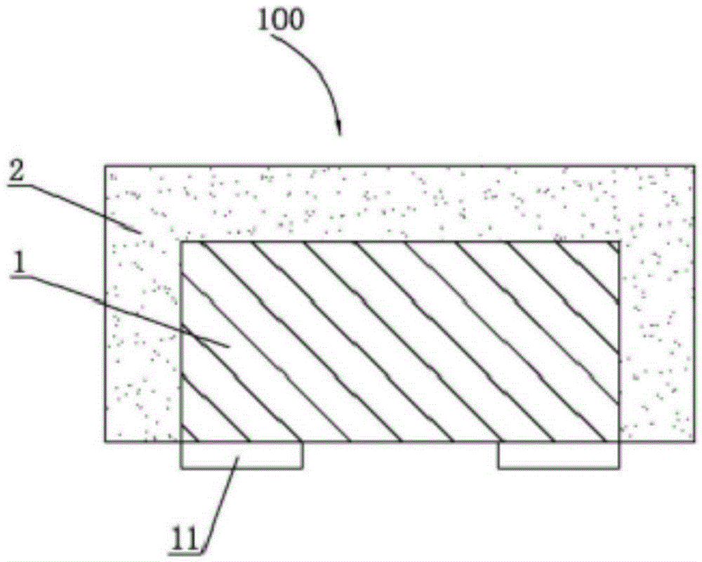
[0059] Such as figure 1 As shown, the LED packaging structure 100 includes a flip chip 1, the flip chip 1 includes a flip chip body and an electrode 11, the electrode 11 is arranged at the bottom of the flip chip body, and the electrode 11 protrudes from the bottom surface of the flip chip body. The side surface and the top surface of the flip chip body are coated with encapsulation glue 2, and the encapsulation glue 2 is fluorescent glue. The lower surface of the encapsulant 2 is higher than the lower surface of the electrode 11 . In this embodiment, the lower surface of the encapsulant 2 is flush with the lower surface of the flip chip body.

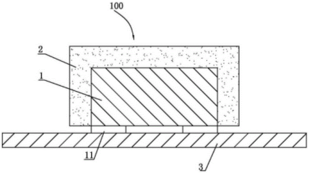
[0060] Such as figure 2 As shown, since the lower surface of the encapsulant 2 is higher than the lower surface of the electrode 11, in the process of fixing the LED package structure 100 to the substrate 3, a space is formed between the lower surface of the encapsulant 2 and the substrate 3, so even if the encapsulation The glue 2...

Embodiment 2

[0062] Such as figure 2 As shown, the LED device includes an LED packaging structure 100 and a substrate 3 .

[0063] The LED packaging structure 100 includes a flip chip 1, the flip chip 1 includes a flip chip body and electrodes 11, the electrodes 11 are arranged at the bottom of the flip chip body, and the electrodes 11 protrude from the bottom surface of the flip chip body. The side surface and the top surface of the flip chip body are coated with encapsulation glue 2, and the encapsulation glue 2 is fluorescent glue. The lower surface of the encapsulant 2 is higher than the lower surface of the electrode 11 . In this embodiment, the lower surface of the encapsulant 2 is flush with the lower surface of the flip chip body.

[0064] Such as figure 2 As shown, since the lower surface of the encapsulant 2 is higher than the lower surface of the electrode 11, in the process of fixing the LED package structure 100 to the substrate 3, a space is formed between the lower surf...

Embodiment 3

[0066] The method for manufacturing the LED package structure of the above-mentioned embodiment 1 is:

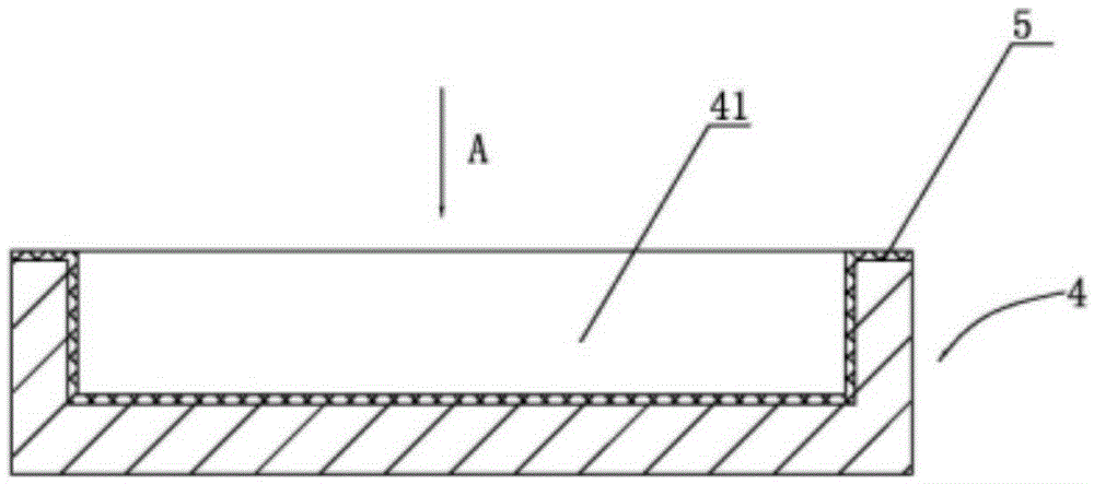
[0067] (1) if image 3 with Figure 4 As shown, a glue-carrying device is provided. In this embodiment, the glue-carrying device is a glue-carrying platform 4. The glue-carrying platform 4 has a glue cavity 41. On the glue-carrying platform, a first isolation film 5 is laid. The first isolation film 5 is a UV film, the thickness of the first isolation film 5 is h 5 . Set the orthographic projection area of ​​the glue chamber 41 as S 1 , the above orthographic projection refers to along image 3 The direction of the projection in the A direction. Such as Figure 4 As shown, the encapsulation glue 2 is injected into the glue cavity 41, the encapsulation glue 2 is a semi-cured glue, the viscosity of the semi-cured glue is 10-80 Pa.s (Pa per second), and the first isolation film 5 will carry the glue The platform is isolated from the packaging glue 2, and the packaging gl...


PUM


Abstract

The invention discloses an LED packaging structure and a manufacturing method. The manufacturing method comprises the steps of providing an adhesive carrying device and a carrier plate, laying a first isolation film and a second isolation film, injecting adhesive, curing, cutting, and separating. The LED packaging structure comprises a flip chip, the bottom of the flip chip is provided with electrodes, the sides and the top of the flip chip are coated with packaging adhesive, and the lower surface of the packaging adhesive is higher than the lower surfaces of the electrodes. An LED packaging structure with a step between the electrodes and the packaging adhesive can be manufactured by the manufacturing method. The hole rate of connection between the LED packaging structure and a substrate is reduced, the fixing reliability of the LED packaging structure is improved, and the reliability of electrical connection between the LED packaging structure and the substrate is improved.

Description

technical field [0001] The invention relates to an LED packaging structure and a manufacturing method. Background technique [0002] The traditional packaging of LED is to fix the chip on the substrate first, and then implement the packaging process on the chip on the substrate. The LED device formed by this packaging process, on the one hand, the chip may move during the packaging process, causing The position accuracy of the chip package is not high, and it will also affect the conductivity of the chip and the substrate. On the other hand, the thickness uniformity of the package glue is difficult to control, resulting in a larger volume and weight of the LED device, which also has a certain effect on light output. influences. For LED devices with multiple chips packaged on the same substrate, such as COB light sources, etc., once the package is completed and the packaged chips are determined, if the chip consistency is not good or some chips are damaged, it will affect T...

Claims


Application Information

Patent Timeline
IPC IPC(8): H01L33/00H01L33/48
CPCH01L33/005H01L33/48H01L2933/0033
Inventor 熊毅李坤锥朱富斌郭生树王跃飞
Owner HONGLI ZHIHUI GRP CO LTD
Why Eureka
Try Eureka