Micro optical communication device package

a technology of optical communication device and micro-optical device, which is applied in the direction of generator/motor, television system, instruments, etc., can solve the problems of long process time, complicated manual work, and affecting the quality so as to facilitate the convenience of optical communication device packages and/or the effect of automation

Inactive Publication Date: 2005-04-14
SAMSUNG ELECTRO MECHANICS CO LTD
View PDF6 Cites 10 Cited by
  • Summary
  • Abstract
  • Description
  • Claims
  • Application Information

AI Technical Summary

Benefits of technology

[0014] It is another object of the invention to provide an optical communication device package which can be fabricated via ultrasonic welding instead of conventional adhesive coating, which suffers from th...

Problems solved by technology

Since the above packaging process is subject to several packaging procedures, the optical device package of the above structure has drawbacks of a long process time and complicated manu...

Method used


Image

  • Micro optical communication device package
  • Micro optical communication device package
  • Micro optical communication device package

Examples


Embodiment Construction

[0034] Hereinafter, preferred embodiments of the present invention will be described in detail with reference to the attached drawings.

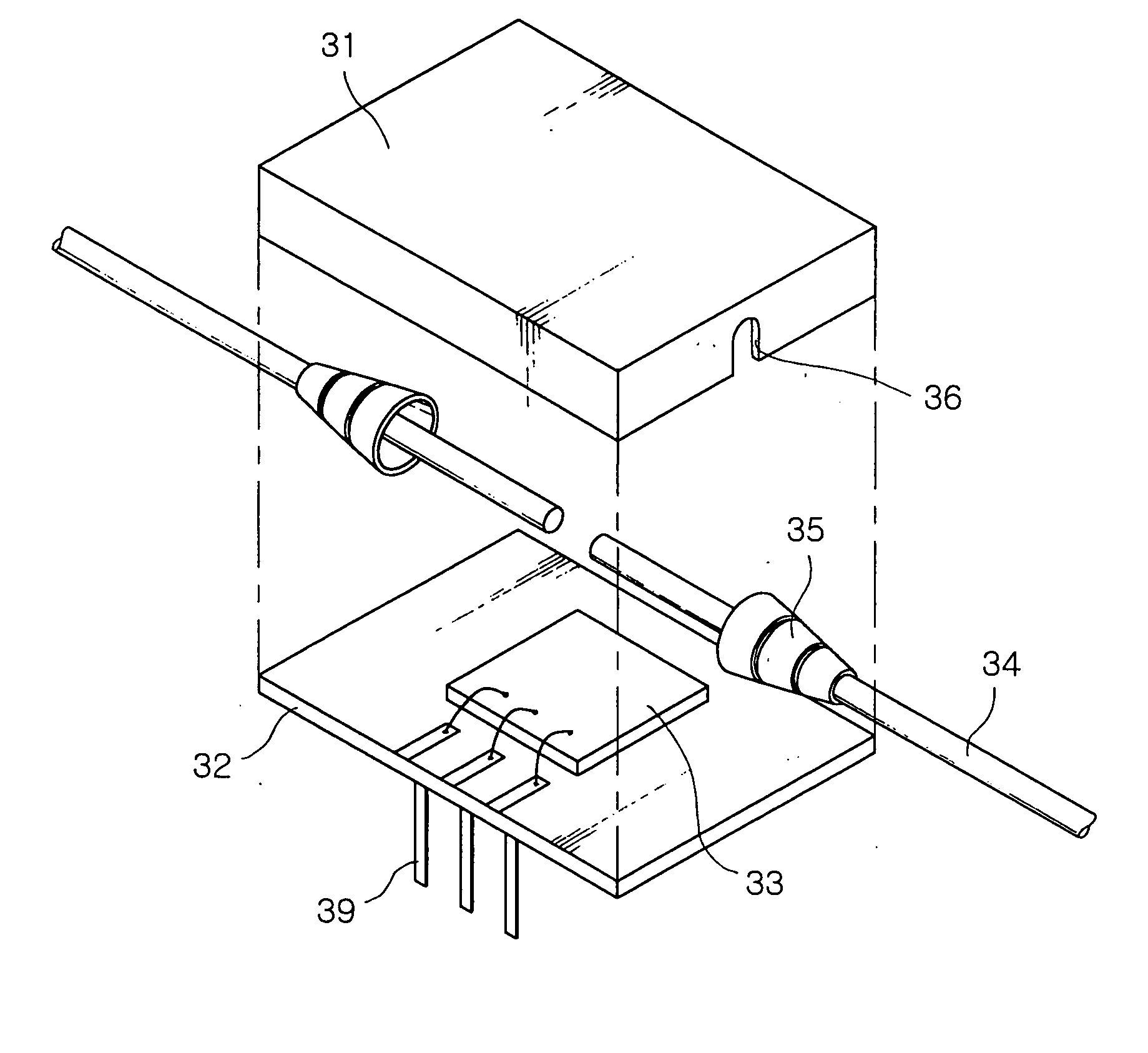
[0035] According to an aspect of the present invention, an optical communication device package of the present invention hermetically seals a MEMS chip with a base for mounting the MEMS chip and an upper housing for covering the base while functioning as an enclosure or housing for containing the MEMS chip.

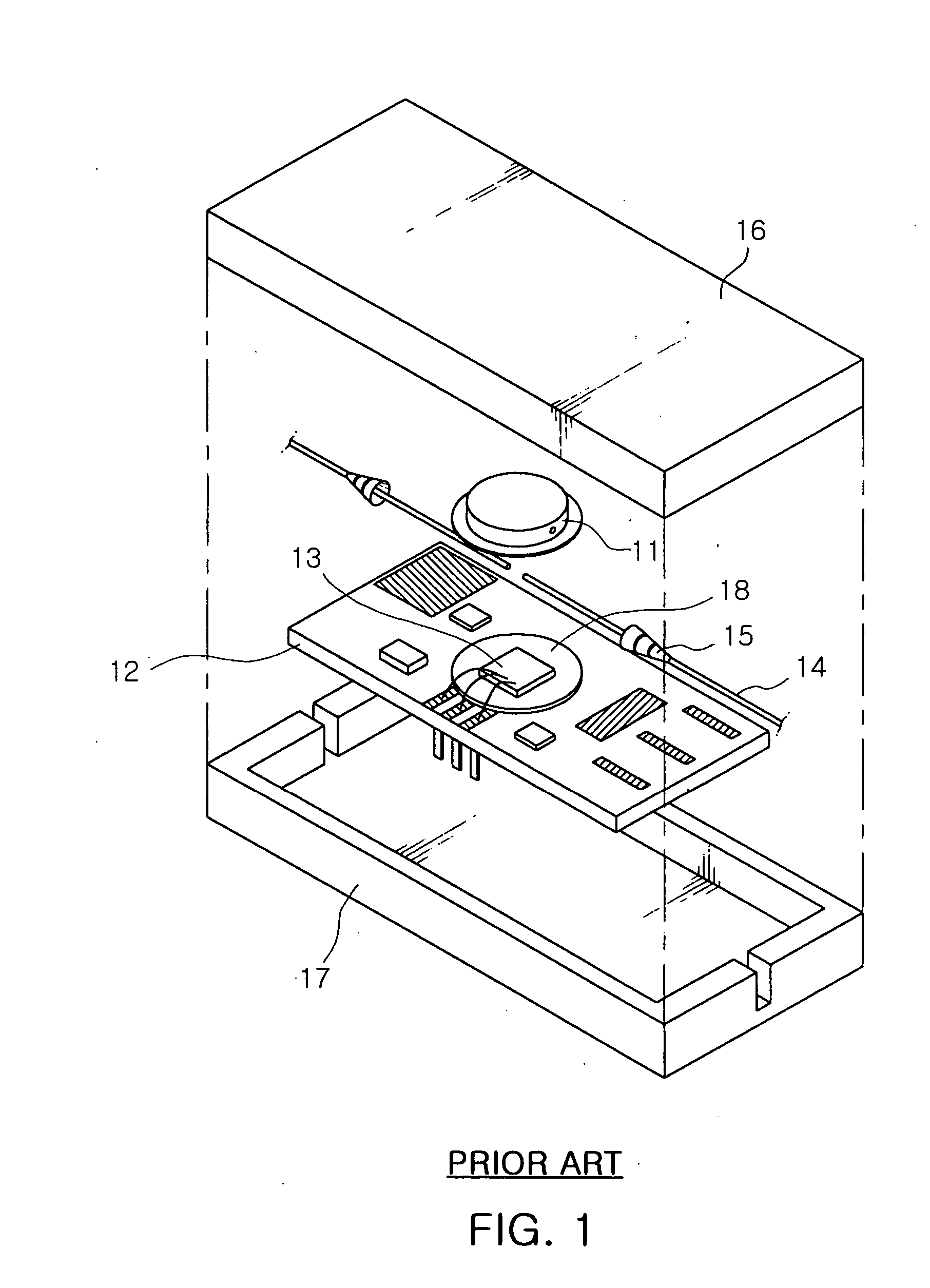
[0036]FIG. 3 is a perspective view illustrating an optical communication device package in accordance with the invention. Referring to FIG. 3, a Micro Electro-Mechanical System (MEMS) chip 33 executing an optical communication function is mounted on a base 32. The MEMS chip 33 is a microscopic chip which is designed to regulate and control a trace amount of light based upon the MEMS Technology. Available examples of the MEMS chip may include an optical attenuator, an optical switch, OADM and so on. Since the MEMS chip 33 contains a microscopic dr...


PUM


Abstract

The present invention relates to a micro optical communication device package. The package of the invention comprises a Micro-Electro-Mechanical System (MEMS) chip for executing an optical communication function. The MEMS chip is mounted on a base. An upper housing having an opened bottom is placed on the base to form an internal space together with the base. The upper housing is sealed with the base to hermetically seal the MEMS chip within the internal space. The MEMS chip is connected an optical fiber, which is extended through the upper housing to form a light path. A boot is fit around the optical fiber and fixed to the upper housing to seal a portion of the upper housing for allowing passage of the optical fiber.

Description

BACKGROUND OF THE INVENTION [0001] 1. Field of the Invention [0002] The present invention relates to a micro optical communication device package based upon the Micro Electro-Mechanical System (MEMS) Technology, more particularly, which combines a hermetic sealing structure for blocking external environment and an outer housing structure into a single housing structure which can hermetically seal the micro optical communication device package while housing the same. [0003] 2. Description of the Related Art [0004] The MEMS Technology incorporates electronic, mechanical and optical technologies to design, fabricate and utilize miniature (microscale or microscopic) components and systems. The MEMS technology can minimize product size through batch production on a wafer based upon semiconductor processing as well as integrate a plurality of functional elements and signal processing modules into a single chip product which has high performance and reliability. [0005] Since the MEMS Techn...

Claims


Application Information

Patent Timeline
IPC IPC(8): G02B6/26B81B7/02G02B6/00G02B6/35G02B6/36G02B6/38G02B6/42G02B26/08H04B10/00H04B10/40H04B10/50H04B10/60
CPCG02B6/3887G02B6/4248G02B6/266G02B6/36G02B6/3582G02B6/3594G02B6/3552G02B6/42
Inventor LEE, YEONG GYULEE, SEONG HUNJUNG, SUNG CHEONPARK, MOO YOUNHONG, SUK KEE
Owner SAMSUNG ELECTRO MECHANICS CO LTD
Why Eureka
Try Eureka