Semiconductor device with integrated circuit electrically connected to a MEMS sensor by a through-electrode

a technology of integrated circuit and integrated circuit, which is applied in the direction of turn-sensitive devices, semiconductor/solid-state device details, instruments, etc., can solve the problem of limitless downsizing and achieve the effect of reducing thickness and downsizing

Inactive Publication Date: 2011-04-05
HITACHI LTD
View PDF16 Cites 12 Cited by
  • Summary
  • Abstract
  • Description
  • Claims
  • Application Information

AI Technical Summary

Benefits of technology

[0011]An object of the present invention is to simplify packaging structure of a semiconductor device including a MEMS sensor and an LSI circuit while achieving both downsizing and thickness reduction and sensitivity enhancement of the semiconductor device including the MEMS sensor and the LSI circuit formed by bulk micromachining techniques such as an acceleration sensor or an angular rate sensor.
[0016]When such a configuration is employed, downsizing and thickness reduction can be realized by forming the LSI circuit (integrated circuit) on one surface of the SOI substrate and forming the MEMS sensor (semiconductor element) on the other surface thereof, compared with the case where the MEMS sensor and the LSI circuit are formed on different semiconductor substrates. In addition, when the MEMS sensor and the LSI circuit are electrically connected to each other by the through-electrodes penetrating through the buried insulating layer, sensitivity and detection accuracy improvement can be achieved.
[0018]In an SOI substrate having a substrate layer, a buried insulating layer buried in the substrate layer, and a silicon layer formed on the buried insulating layer, an LSI circuit is formed on the silicon layer, and on the other hand, a MEMS sensor is formed by processing the substrate layer. In other words, the LSI circuit is formed on one surface of the SOI substrate, and the MEMS sensor is formed on the other surface thereof, thereby realizing downsizing and thickness reduction compared with the case where the MEMS sensor and the LSI circuit are formed on different semiconductor substrates.
[0020]Furthermore, external draw-out electrodes can be provided in the side where the LSI is formed also in the case where the structure constituting the MEMS sensor is hermetically sealed; therefore, there is no need to form opening portions in a cap hermetically sealing the structure to form external draw-out electrodes. Consequently, the step of hermetically sealing the structure configuring the MEMS sensor can be simplified, and reliability of the bonding surfaces of the cap and the MEMS sensor can be improved.

Problems solved by technology

Therefore, downsizing has a limit.

Method used


Image

  • Semiconductor device with integrated circuit electrically connected to a MEMS sensor by a through-electrode
  • Semiconductor device with integrated circuit electrically connected to a MEMS sensor by a through-electrode
  • Semiconductor device with integrated circuit electrically connected to a MEMS sensor by a through-electrode

Examples


first embodiment

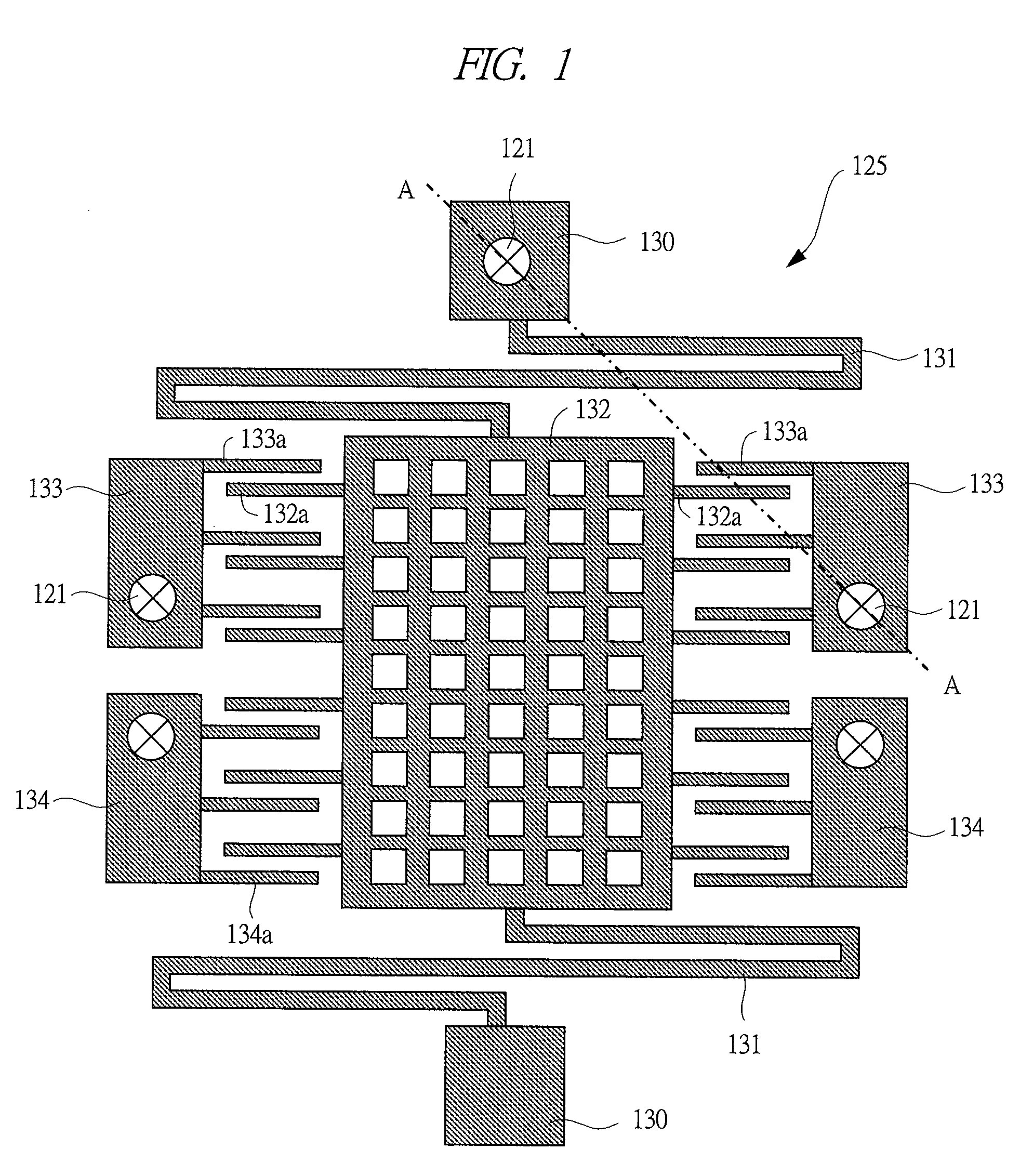
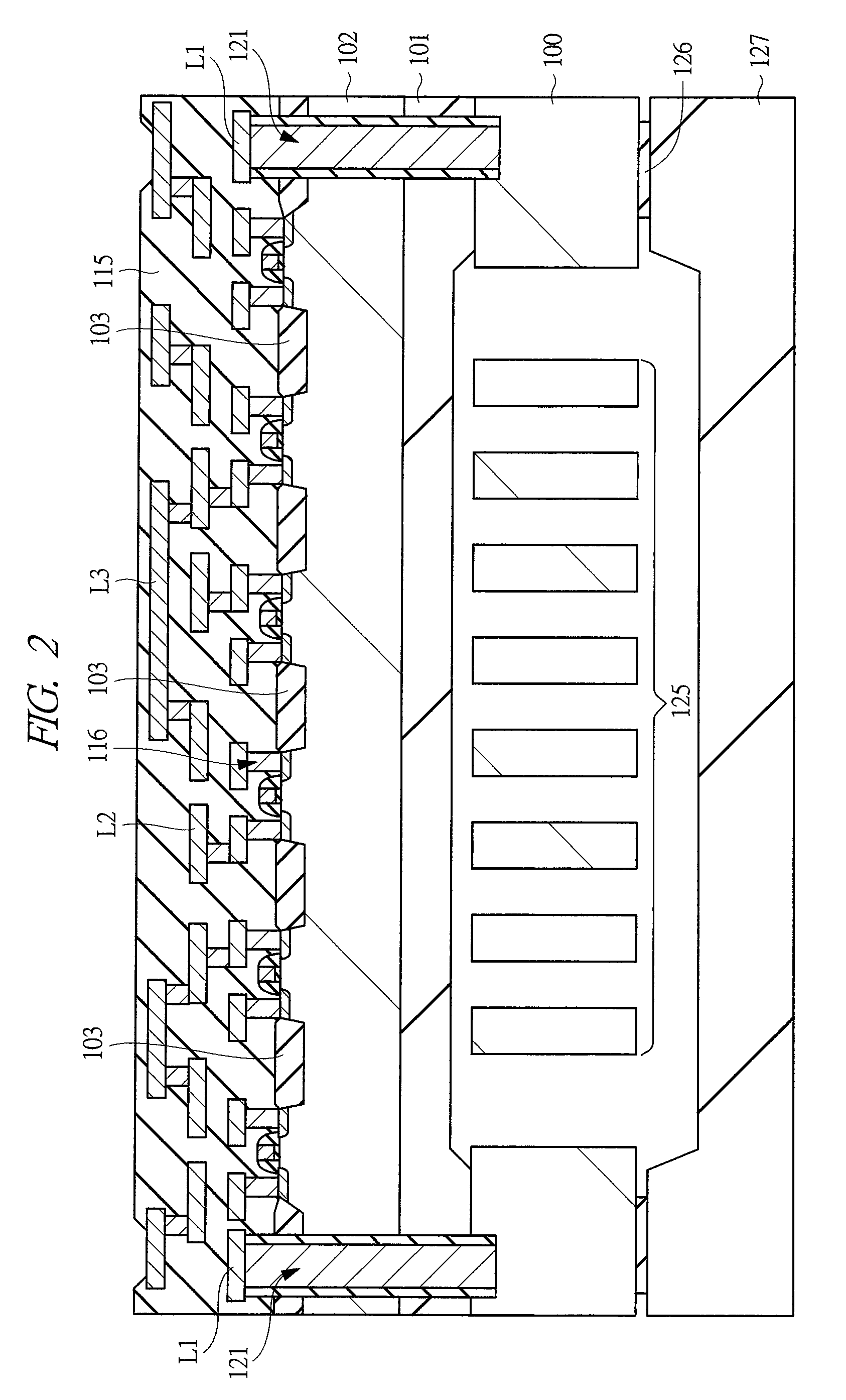
[0060]A semiconductor device of a first embodiment will be described with reference to the drawings. FIG. 1 is a plan view showing a MEMS sensor according to the first embodiment. In FIG. 1, the MEMS sensor in the present first embodiment is, for example, an acceleration sensor. The MEMS sensor comprises fixing portions 130 formed on an SOI substrate and a structure 125 connected to the fixing portions 130. The structure 125 comprises beams 131, a movable mass 132, and detection portions 133 and 134.

[0061]The beams 131 are elastically deformable and connect the fixing portions 130 and the movable mass 132. Therefore, the movable mass 132 can be displaced when an external force is applied. The fixing portions 130, the beams 131, and the movable mass 132 are formed by processing conductive silicon, and are not only mutually mechanically connected, but also are electrically connected.

[0062]Movable electrodes 132a are formed on the movable mass 132 and constitute detection capacitor ele...

second embodiment

[0123]In a second embodiment, an example of using a substrate in which a plurality of buried insulating layers are formed as an SOI substrate will be described. The second embodiment is different from the abovedescribed first embodiment in a point that the SOI substrate in which the plurality of buried insulating layers are formed is used and a point that a plurality of through-electrodes having different connection destinations are formed in the SOI substrate.

[0124]First of all, a MEMS sensor of the second embodiment is an angular rate sensor. A configuration of the angular rate sensor will be described with reference to FIG. 18.

[0125]FIG. 18 is a plan view showing the configuration of the angular rate sensor which is the MEMS sensor. In FIG. 18, the angular rate sensor of the second embodiment has fixing portions 253 formed on the SOI substrate and the structure 125 to be connected to the fixing portions 253. The structure 125 has movable masses 250 and 251 and detection portions ...


PUM


Abstract

As well as achieving both downsizing and thickness reduction and sensitivity improvement of a semiconductor device that has: a MEMS sensor formed by bulk micromachining technique such as an acceleration sensor and an angular rate sensor; and an LSI circuit, a packaging structure of the semiconductor device having the MEMS sensor and the LSI circuit can be simplified. An integrated circuit having MISFETs and wirings is formed on a silicon layer of an SOI substrate, and the MEMS sensor containing a structure inside is formed by processing a substrate layer of the SOI substrate. In other words, by using both surfaces of the SOI substrate, the integrated circuit and the MEMS sensor are mounted on one SOI substrate. The integrated circuit and the MEMS sensor are electrically connected to each other by a through-electrode provided in the SOI substrate.

Description

CROSS-REFERENCE TO RELATED APPLICATION[0001]The present application claims priority from Japanese Patent Application No. JP 2007-297854 filed on Nov. 16, 2007, the content of which is hereby incorporated by reference into this application.TECHNICAL FIELD OF THE INVENTION[0002]The present invention relates to a semiconductor device and a manufacturing technique of the same, and more particularly, it relates to a technique effectively applied to a semiconductor device that includes a MEMS (Micro Electro Mechanical Systems) and an LSI (Large Scale Integrated circuit) and manufacturing techniques of the same.BACKGROUND OF THE INVENTION[0003]In Japanese Patent Application Laid-Open Publication No. 2005-169541 (Patent Document 1), there is described a structure of an acceleration sensor in which a MEMS chip having a MEMS formed therein and an IC chip having an IC (Integrated Circuit) formed therein are arranged so as to oppose to each other at a predetermined spacing therebetween. Particu...

Claims


Application Information

Patent Timeline
Patent Type & Authority Patents(United States)
IPC IPC(8): H01L27/12B81B3/00G01C19/56G01C19/5747G01C19/5769G01P15/125H01L21/3205H01L21/336H01L21/768H01L21/8234H01L23/522H01L27/00H01L27/06H01L27/08H01L27/088H01L29/786H01L29/84
CPCB81C1/00246H01L21/76898H01L23/481B81B2201/0235B81C2203/0778B81C2203/0728H01L2924/0002B81C2203/0735H01L2924/00012H01L2924/00
Inventor GOTO, YASUSHIFUJIMORI, TSUKASAJEONG, HEEWONYAMANAKA, KIYOKO
Owner HITACHI LTD
Why Eureka
Try Eureka