Lateral high-voltage device

a high-voltage device, lateral technology, applied in the direction of semiconductor devices, electrical apparatus, transistors, etc., can solve the problem of not further relieve the contradiction between the breakdown voltage bv, and achieve the effect of reducing the specific on-resistance ron, reducing the surface area, and keeping the character of withstanding voltag

Inactive Publication Date: 2018-09-04
UNIV OF ELECTRONICS SCI & TECH OF CHINA
View PDF8 Cites 12 Cited by
  • Summary
  • Abstract
  • Description
  • Claims
  • Application Information

AI Technical Summary

Benefits of technology

[0019]The advantages of the present embodiments: by introducing the dielectric trench region in the drift region, the device can keep the character of withstanding voltage, reduce the surface area and reduce the specific On-Resistance RON,sp; in the device drift region, a cascade of P-type heavy doping pillars and N-type heavy doping pillars are introduced to provide a low resistance conductive pathway for the on state of the device, which can further reduce the specific On-Resistance RON,sp of the device, and finally achieve the purposes of effectively reducing the device area and reducing the specific On-Resistance RON,sp.

Problems solved by technology

The contradiction between the breakdown Voltage BV and the specific On-Resistance Ro N, is the problem of “Silicon Limit” in the industry.
However, the traditional dielectric trench LDMOS still has a large specific On-Resistance RON,sp, which could not further relieve the contradiction between the breakdown Voltage BV and the specific On-Resistance RON,sp.

Method used


Image

  • Lateral high-voltage device
  • Lateral high-voltage device
  • Lateral high-voltage device

Examples


embodiment 1

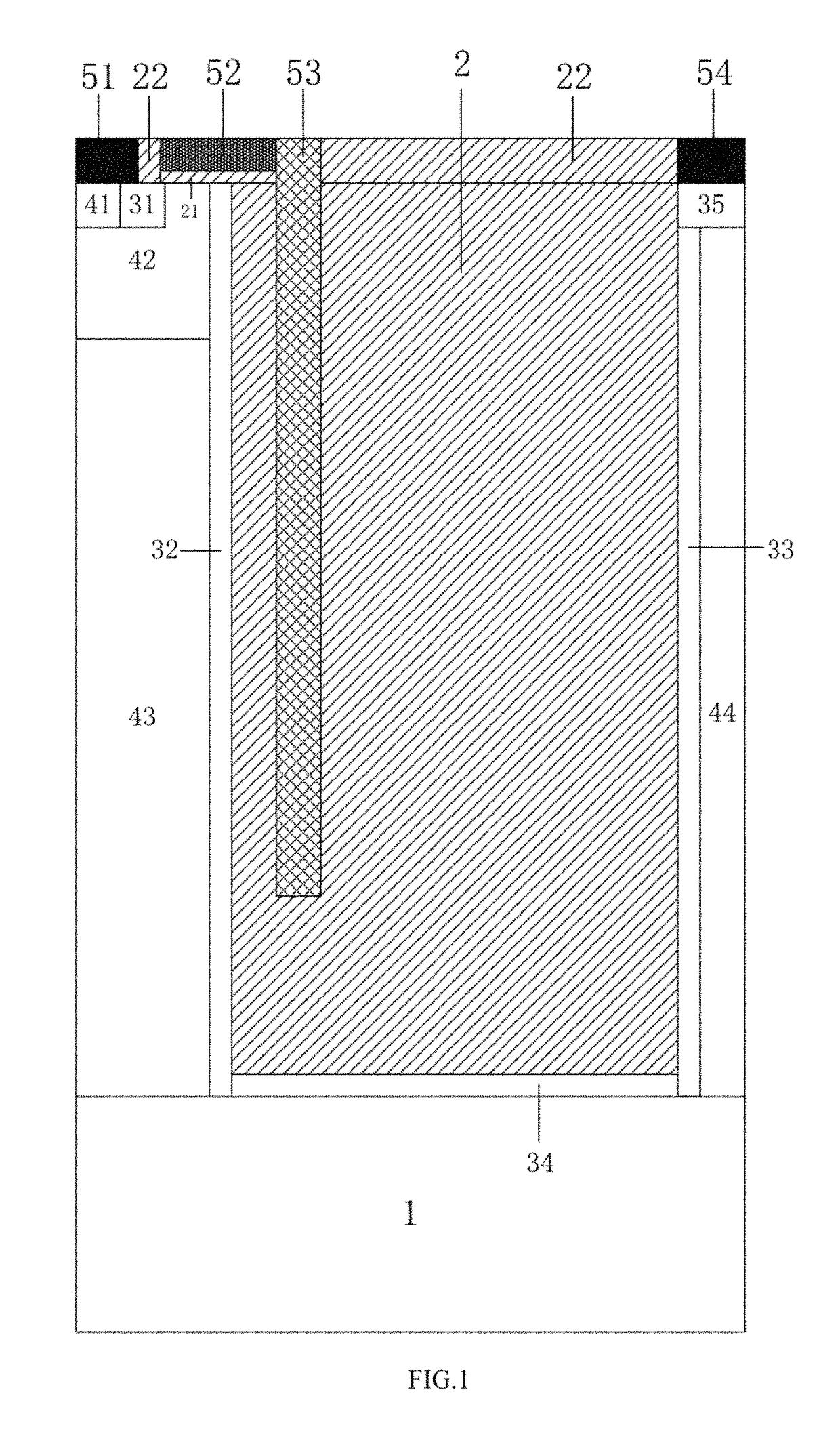
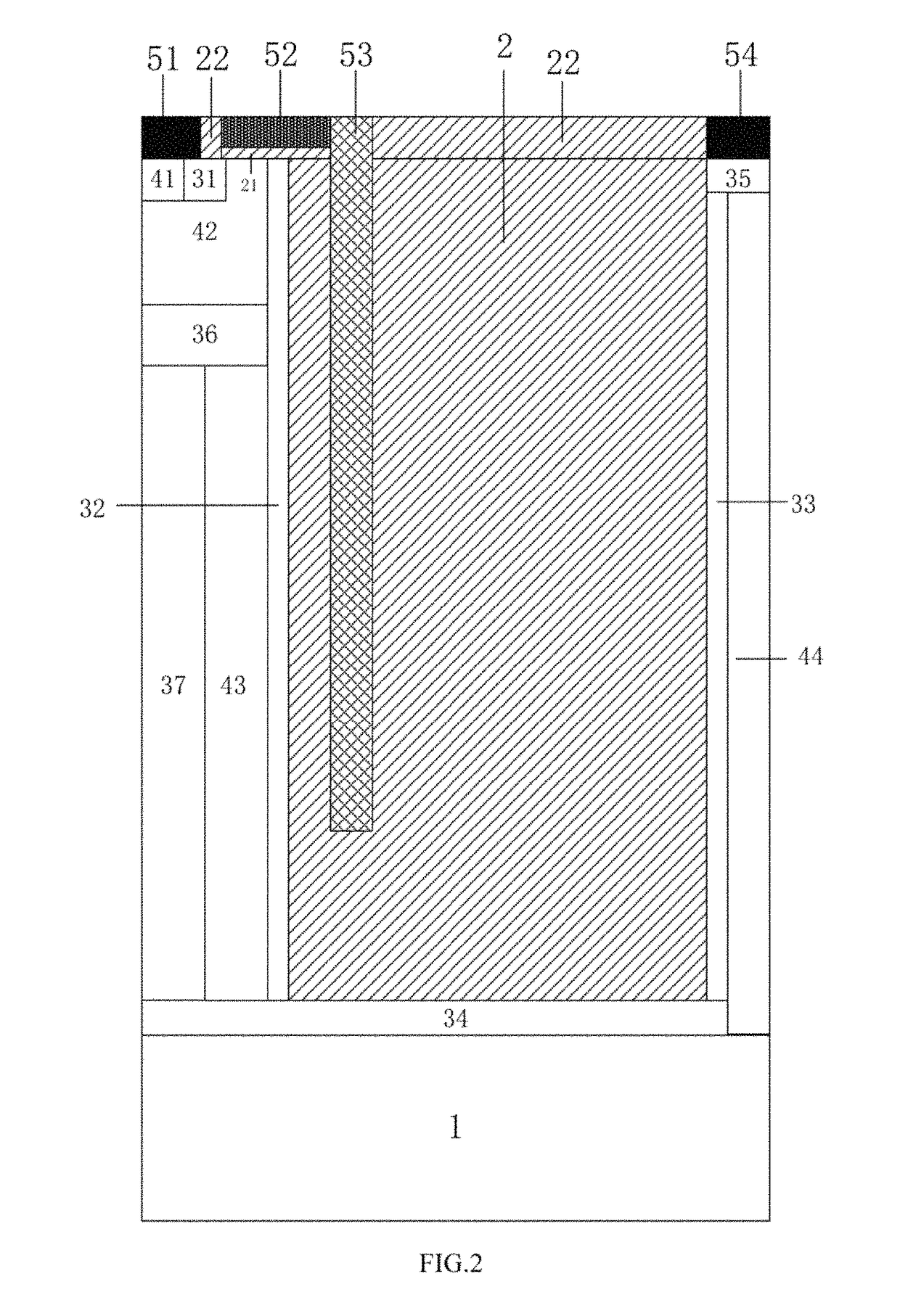
[0043]As shown in FIG. 2, a lateral high-voltage device, comprising: a dielectric trench region 2, a doping-overlapping structure with different doping types in an alternating mode is provided on the left side of the dielectric trench region 2. The doping-overlapping structure includes the first N-type doping pillar 32, the first P-type doping pillar 43 and a fifth N-type doping pillar 37, and there is a fourth N-type doping pillar 36 between the doping-overlapping structure and the P-well region 42. The upper surface of the dielectric trench region 2 is a dielectric layer 22, and a body field plate 53 extends from the surface of the device to the interior of the dielectric trench region 2. The body field plate 53 is adjacently connected to a polysilicon gate 52, the gate oxide layer 21 is located below the polysilicon gate 52. A source contacting terminal 51 and the polysilicon gate 52 are isolated through the dielectric layer 22. The body field plate 53 and a drain contacting term...

embodiment 2

[0048]As shown in FIG. 3, the embodiment 2 and embodiment 1 are essentially the same, except that: the doping-overlapping structure is on the right side of the dielectric trench region 2. When the doping-overlapping structure is on the right side of the dielectric trench region 2, the doping-overlapping structure sequentially includes the second N-type doping pillar 33, the second P-type doping pillar 44 and the seventh N-Type doping pillar 39. The upper surfaces of N-type doping pillar 33, P-type doping pillar 44 and N-type doping pillar 39 contact with the second N-type heavy doping region 35.

embodiment 3

[0049]As shown in FIG. 4, the embodiment 3 and embodiment 1 are essentially the same, except that: the doping-overlapping structure is below the dielectric trench region 2. When the doping-overlapping structure is below the dielectric trench region 2, the doping-overlapping structure sequentially includes the third N-type doping pillar 34, the third P-type doping pillar 45 and the sixth N-type doping pillar 38.


PUM


Abstract

The present invention relates to a lateral high-voltage device. The device includes a dielectric trench region. A doping-overlapping structure with different doping types alternating mode is provided at least below, on a left side of, or on a right side of the dielectric trench region. The device also includes a dielectric layer, a body field plate, a polysilicon gate, a gate oxide layer, a first N-type heavy doping region, a second N-type heavy doping region, a P-type heavy doping region, a P-well region, the first N-type doping pillar, the second N-type doping pillar, the third N-type doping pillar, the first P-type doping pillar, and the second P-type doping pillar. The invention adopts a dielectric trench region in the drift region to keep the breakdown voltage BV of the device while reducing the surface area of the device, and effectively reducing the device's specific On-Resistance RON,sp.

Description

CROSS REFERENCE[0001]The present application is based on, and claims priority to Chinese application numbers CN201710495848.X and CN2017104967120, both filed on Jun. 26, 2017, the disclosures of which are hereby incorporated by reference in their entirety.TECHNICAL FIELD[0002]The present invention relates to semiconductor power devices, particularly relates to a lateral high-voltage device.BACKGROUND[0003]As a core device in PIC (Power Integrated Circuit), a power LDMOSFET (Lateral Double-diffused Metal-Oxide-Semiconductor Field Effect Transistor) has the advantages of easy integration, low drive power and negative temperature coefficient, and has been developing for many years in the direction of high breakdown Voltage (BV) and lower specific On-Resistance (RON,sp). The higher breakdown Voltage BV requires that the device has a longer drift region length and a lower drift region doping concentration, which leads to a higher specific On-Resistance RON,sp. The contradiction between t...

Claims


Application Information

Patent Timeline
Patent Type & Authority Patents(United States)
IPC IPC(8): H01L29/06H01L29/78H01L27/02H01L29/40H01L29/739H01L29/735
CPCH01L29/063H01L29/7816H01L27/0266H01L29/408H01L29/739H01L29/402H01L29/735H01L29/407H01L29/7824H01L29/7825H01L29/0634H01L29/0653H01L29/0878H01L29/0882H01L29/0886H01L29/7394
Inventor QIAO, MINGYU, YANGZHANG, WENTONGWANG, ZHENGKANGZHAN, ZHENYAZHANG, BO
Owner UNIV OF ELECTRONICS SCI & TECH OF CHINA
Why Eureka
Try Eureka